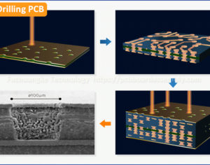
Key Processing Factors of HDI PCB Manufacturing

High Density Interconnect (HDI) Printed Circuit Board (PCB) Manufacturing is always related to the processing of micro vias, especially Staggered Micro Via and Stacked Micro Via. At the same time, Staggered and Stacked vias have significant effect on the development of HDI PCB design and HDI board manufacturing technology.
Click to check our advanced HDI PCB Manufacturing Capabilities.
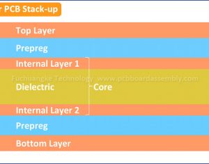
Micro Via
Also called as Microvia, a blind or buried hole that is less than or equal to 0.15 mm (6mils) in diameter having a pad diameter that is less than 0.35mm (13.8 mils) formed by laser or mechanical drilling, wet/dry etching, photo imaging or conductive ink-formation followed by a plating operation. Micro vias connect an outer layer of a PCB board to the nearest inner layer. These vias are small and can be placed on the pads (via-in-pad), PCB designers get to have more routing room which allows them to increase circuit density and routing capacity for electronic products that are smaller and lighter.
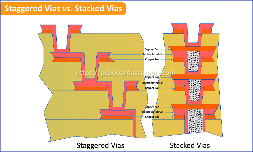
Staggered Via, or Staggered Micro Via, is a type of compound design made by placing micro-via with small offsets from each other between layers. This is the most reliable complex design structure but it requires slightly more space in the HDI PCB design. Staggered via is an order of magnitude more robust than stacked via.
Stacked Via, or Stacked Micro Via, is usually designed when routing density is extreme and even staggered via buildup doesn’t solve the rising connection demand problem. This via can be used to achieve the highest possible routing density and come up with high-density packaging, and reduce the PCB size and PCB layer count as much as possible.
Microvia Filling Process
The stacked micro via must be filled and has a copper cap on the micro via or buried via upon which the micro via is stacked. One of the areas of concern with stacked via is that the HDI PCB Manufacturer produces an electrical path that includes the copper cap in the structure upon which the micro via is stacked. By this, the copper cap is not part of the circuit until the PCB producer stack another structure on top of it.
In stacked structures, not only do microvias and buried vias have caps–they also must have a fill upon which the copper cap is formed. They usually include a planarization step to reduce the copper thickness and assure a good electrical contact with the plated copper wrap. There are 3 types of fills currently in HDI PCB fabrication. The fill may be electrolytic copper plating, an “a-stage” fill, which is the liquid of the dielectric system. Or a third-party epoxy fill. The electrolytic copper plating is good; barrel crack failures are precluded because the whole micro via (or rarely, the buried) is solid copper. The “a-stage” fill is good because the “a-stage” has the exact attributes, glass transition temperature (Tg) and coefficient of thermal expansion (CTE) of the base dielectric material. The third-party fill may be conductive or non-conductive, but it does not have the same material characteristics, Tg and CTE as the base material. Each type of fill has its own advantages and disadvantages.
Planarization Process
Planarization is an HDI PCB fabrication process where the fill and some of the copper associated with the wrap is removed from the knee of the microvia or buried via to reduce the copper thickness between layers and make a good connection between the electroplated cap and the copper wrap. If the planarization is not aggressive enough, there may be a problem with conductivity between the wrap and the cap leading to an open circuit. If the planarization is too aggressive, there is a problem where the wrap is too thin and this can lead to damage due to the knee cracks.
There is a problem with the third-party fills in that they frequently have a different Tg and a different CTE than the epoxy of the base dielectric layers. When these are used to fill the buried vias or microvias, there can be problems due to these differences.
CTE Consideration
HDI board manufacturer should consider the CTE, which is is one of the factors that create a mismatch between the fill and the dielectric material used to fabricate the HDI board. The CTE of the base dielectric material is usually around 30-80 ppm/°C before Tg, and it can be as high as 400 ppm/°C after Tg. The fill material will frequently have a CTE of 40-80 ppm/°C before Tg, and 120 ppm/°C to 160 ppm/°C after Tg. The copper in the barrel of the hole usually has a CTE from 11 ppm/°C to 17 ppm/°C. There is a mismatch between the CTE of the third-party fill, the copper barrel and the dielectric.
One of the ways to calculate Tg is when the CTE of the material changes. Usually the Tg of the third-party fill is less than the Tg of the dielectric. The typical high-end dielectric will have a Tg of 170°C. The Tg of the filler material is between 120°C and 160°C. In the case of the lower Tg of the filler when compared to the Tg of the material, this means the higher rate of thermal expansion of the fill material will be occurring before the higher rate of expansion changes based on the Tg of the base dielectric material. During the thermal excursions that the board is exposed to during assembly and rework, this difference in Tg makes the fill in the buried via expand at a higher rate than the dielectric for the time it takes the board to reach the Tg of the base dielectric material.
The dielectric base material is usually fiber glass reinforced constricting the x and y axis expansion of the base material, but there is little constraint in the z axis. The third-party fill has no fiberglass and therefore has equal expansion in the x, y and z axes.
Consider the third-party fill inside the microvia or the buried via. It is expanding in the three axes at, let’s say, 160 ppm/°C. But how much it expands, the overall length of expansion, is a function of the thickness of the fill in that particular axis. The layers of copper and glass tend to reduce the CTE in the area around the PTH.
HDI PCB Quote and HDI PCB Assembly Quote
Here are FR4 HDI PCB Quote, HDI Flexible PCB Quote and HDI Rigid-Flex PCB Quote.
FR-4 PCB Quote Flexible PCB Quote Rigid-Flex PCB Quote