With increasing demand of miniaturization and high integration of electronic products, more and more PCB layout designs adopt blind and buried vias technology to improve circuit density of PCB boards. PCBs with blind and/or buried vias have more space to wiring than standard PCBs. And blind and buried vias are widely used in multilayer printed circuit boards manufacturing.
Via Hole
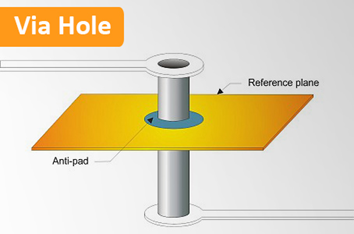
A via hole in a PCB is a copper through-plated hole, which consists of 2 pads in corresponding positions on different layers of the circuit board, that are electrically connected by a hole through the board. The hole is made conductive by electroplating.
- Barrel: conductive tube filling the drilled hole
- Pad: connects each end of the barrel to the component, plane or trace.
- Anti-pad: clearance hole between barrel and no-connect metal layer

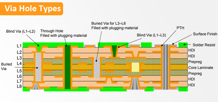
Blind Vias
Connects an outer layer to one or more inner layers but does not go through the entire board, and they are visible from the one outer layer but not visible from the other outer layer.
Buried Vias
Connects two or more inner layers but does not go through to an outer layer, and they are not visible from any one of the outer layers.

Blind and buried vias are used to connect between layers of a printed circuit board where space is at a premium. But not all combinations are possible. It is specified by UL (Underwriters Laboratories) that three thermal press cycles are the maximum. Thus, for maximum reliability and quality we cannot produce multi-layer PCB boards that require more than 3 lamination steps. What this means is you may bot design vias in such a way that it would take more than 3 steps to assemble them. Besides, blind and buried vias add considerably to the cost of a circuit board. They should only be used when absolutely necessary. To help PCB designers of tight printed boards, we offer via holes down to 0.2mm, and microvia down to 0.1mm(4mil). These need minimum outer layer pad sizes of 0.45mm and 0.4mm respectively.
Blind and Buried Vias Manufacturing Capabilities
We use combination of depth-controlled laser drilling and mechanical NC drilling to manufacture the blind and/or buried vias. The blind and buried vias manufacturing capabilities for standard PCBs and HDI PCBs as following.

| Via Type | Via Diameter (max) |
Via Diameter (min) |
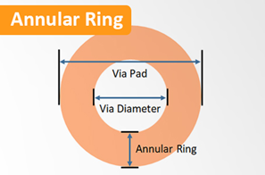
Via Pad | Annular Ring | Aspect Ratio |
| Blind via (mechanical) | 0.4mm | 150µm | 450µm | 127µm | 1:1 |
| Blind via (laser) | 0.1mm | 100µm | 254µm | 150µm | 1:1 |
| Buried via (mechanical) | 0.4mm | 100µm | 300µm | 150µm | 1:10 |
| Buried via (laser) | 0.4mm | 100µm | 225µm | 150µm | 1:12 |
Check to know more
Flexible Circuits & Rigid-Flex PCB Capabilities
Advantages
- Increasing wiring layout density and saving PCB space.
- Reduction of layer count by widening the BGA breakout channel with a blind via.
- Elimination of electrical layers by replacing through-hole vias with microvias
- Reduction of PCB aspect ratio (PCB thickness /Drilled Hole Diameter)
FR-4 PCB Quote Flexible PCB Quote Rigid-Flex PCB Quote IMS PCB Quote