8 Factors That Affect Multilayer PCB Cost
When PCB layer count comes to or bigger than 3 layers, the board is defined as a multilayer printed circuit board (PCB). As a PCB manufacturer, our standard manufacturing capabilities support 4-layer to 20-layer multilayer PCB fabrication. But what are the factors to affect a multilayer PCB cost? Read on to learn more.
PCB Materials
The first one is rather obvious, which is the materials that the multilayer PCB manufacturer will use to fabricate your PCB board. The PCB materials used in a circuit board will invariably affect its cost. It is understandable due to the type of manufacturing materials in use affects the cost of nearly everything within every industry. The main multilayer PCB materials are laminated together to build your board are listed below,
| FR4 PCB | FR4 CCL, RCC, Copper Foil, Prepreg (PP) |
| MCPCB | Metal Core Based Laminate, like Aluminum, Copper; Prepreg (PP) |
| FPC | PI FCCL, Adhesive, Prepreg (PP), Coverlay |
Here are the 5 considerations when choosing the right PCB base material to fabricate your multilayer PCB boards.
- Thermal Reliability: Excellent thermal reliability requirements are critical in nowadays certain electronics and devices, like vehicle electronics. Will your multilayer PCB board survive through higher-temperature lead-free reflow soldering assembly without defects, such as blisters or delamination? Will your PCB assembly hardware be capable of stably operating over its lifetime under certain working environment? Certain PCB boards require PCB materials of a higher thermal rating than standard PCBs.
- Glass Transition Temperature: Can the material withstand an expected range of temperature conditions within a controlled setting without overheating? If multilayer PCBs designed for high-temperature working operations, can you ensure the PCBs will not be reliable? Certain multilayer PCB manufacturing requires copper clad laminate (CCL) and PP materials with high glass transition temperature, like >=Tg170. If choosing low Tg materials, the resin in them will be de-laminated, then the vias will be broken, and the electrical connectivity will be broken.
- Thermal Conductivity: Will the multilayer PCB boards withstand high-intensity loads without transferring undue levels of heat to attached and adjacent components? Taking LED PCB as example, if the thermal conductivity of the base material is low, the SMD LED brightness and life will be reduced when works under the high-temperature environment in long time. Generally, FR4 thermal conductivity is around 0.25W/m·K.
- Signal Performance: Will the PCB material facilitate uninterrupted electrical signals throughout each operating cycle of a given product? Will the signal withstand a necessary range of temperatures and other environmental factors? These concerns are integral to the performance of a multilayer PCB. As you know, this is critical to the PCBA functionality.
- Mechanical Properties: It is the deciding factor to the material’s ability to withstand the foreseeable physical stresses of its application use. FR-4 is the most commonly used as an electrical insulator processing considerable high mechanical strength in both dry and humid conditions. Does the PCB material used to build your multilayer PCB board have sufficient physical composition to withstand the mechanical processing? like tight routing without cracking.
PCB Size
All PCB base materials have their dimensions, like lengths and widths. If your multilayer PCB board is not big enough, the PCB manufacturer will panelize a few single boards in a set, and panelize a few sets to a working panel to fit the base materials’ dimensions. Base materials are charged by dimension, so the PCB pricing is some certain CNY per square meter for mass production. For PCB prototypes, this calculation is not applicable.
This is not to recommend you to design a tiny or a small PCB board, just let you know the size of your single board and its panel utilization are two of the most crucial factors that affect the multilayer PCB cost. In some applications, the PCB size can be very small, like an USB flash disk. But for some other applications, the PCB size are large, like industrial machinery. But for tiny board, the outline routing paths in a set or a panel must be longer that of a large PCB. The routing time and labor cost will be comparatively higher. That’s to say, not smaller, the cheaper. Except for PCB size, we also need to concern other processes time consumption.
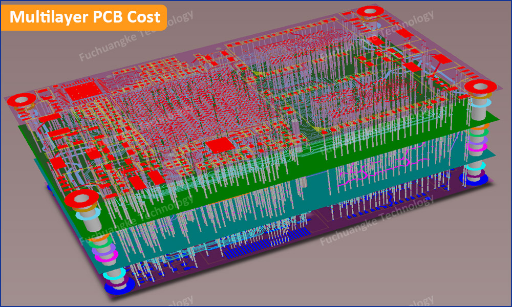
PCB Layer Count
The common sense is that the more layers, the higher the cost. It’s easy to understand. A double-sided PCB board no need copper foil lamination and more outer layers processing, but for a four-layer PCB, it requires these extra processes. PCB layer count is also one of those distinct determining factors of mutilayer PCB cost. Some professional on internet gives a general comparison of the multilayer PCB cost increases between different layer count. You can read it below, but please note it doesn’t stand for all situations, just let you know how layer count increases the PCB cost.
2-Layers to 4-Layers: 35%-40% PCB cost increase
4-Layers to 6-Layers: 30%-40% PCB cost increase
6-Layers to 8-Layers: 30%-35% PCB cost increase
8-Layers to 10-Layers: 20%-30% PCB cost increase
10-Layers to 12-Layers: 20%-30% PCB cost increase
One of the most significant multilayer PCB price increases in the manufacturing process occurs when you add a second layer. This is understandable since we know that this increases the number of production processes (or lamination process). The logic here is, the more layers, the more time and resources are required to complete the manufacturing process.
Surface Finish (OSP, HALF, ENIG, etc.)
The surface finish you choose for your multilayer PCB design will also affect the PCB cost, but it is a minor factor; some finishes boast higher grade and offer longer shelf life, thus adding to the overall cost of production. One of the more common and low-cost surface finish is HASL lead free (HALF), which offers good solderability but is rated unfavorable on other counts.
ENIG, by comparison, scores favorably in most categories yet only commands a slight price difference. But need to consider the ENIG covering surface on a PCB board. The multilayer PCB manufacturer charges the ENIG cost as per the coverage rate not more than 20%. If more than it, the ENIG cost will be higher.
In some HDI PCB designs, the customers require multiple surface finish, like OSP + ENIG, which is the most commonly used in HDI board manufacturing. Yes, two different surface finishes are applied on the same board. The OSP is applied on the fine pitch BGA areas, and ENIG is applied on other areas for reducing BGA assembly defects and improving the electrical connectivity.
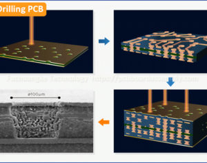
Hole Size, Hole Density & Hole Type
- Hole Size: The hole size will impact the final cost of multilayer PCB production. Standard aspect ratio of rigid board is 8:1. If board thickness is 1.6mm, the manufacturable mechanical drilling diameter is 0.2mm. But you want 0.15mm mechanical drilling on 1.6mm, then multilayer PCB manufacturer need customized tools to produce it.
- Hole Density: What’s PCB hole density? It’s the hole quantity per square meter, which is also applicable for laser drilling. Generally, the hole density less than 120Kpcs/sqm is normal. If more than it, multilayer PCB manufacturer need increase drilling cost into the PCB cost.
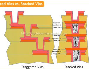
- Hole Type: Mechanical drilling has 4 types, including thru-hole, back-drilling, blind and buried vias. Thru-holes is understandable, no price increases. But when you board has back-drilling, blind and buried vias, it will increase the hole processing steps, the to increase the multilayer PCB cost.
Min Trace Width and Spacing
Engineers know if you want to transfer current on a multilayer PCB without overheating it or damage it, you must have sufficient trace width. Regardless of board size, there is a general correlation between trace width and current carrying capacity. Although other factors affect current carrying capacity, the need for wider (thicker) traces will require more materials and work. Again, this will equate to an increase in multilayer PCB price.
It must be noted that trace carrying capacity does not necessarily correspond to the cross-section space. In fact, the amount of current that a trace can hold, at maximum, cannot be easily calculated, regardless of the trace width or temperature rise. The carrying capacity of a current can also be impacted by pads, vias and other board elements.
On a multilayer PCB board with numerous pads, you might encounter a trace of exceptional capacity. If this is not accounted for in the soldering process, an excessive cross-sectional are might be created, and transient surges are liable to occur. To avoid this situation, board makers will enlarge the trace width, if possible, Alternately, they can add extra solder mask to the traces that might otherwise be prone to burn. These steps can add to the price of a multilayer PCB production.
PCB Thickness
Until recently, the thickness of a multilayer PCB has played only a minor role in the overall cost, though all that is liable to change in the coming years. Thicker material can be costlier to produce, laminate and form into a printed circuit board, especially if the design itself is highly intricate.
Thinner materials will generally put a line of multilayer PCBs into a slightly lower cost bracket because less material is required for the production at hand. The costs of a board in regards to thickness can also be impacted by the type of material used in a given production.
The standard thickness for a multilayer PCB is 1.6mm (0.063’’). In recent times, ticker boards have become more expensive, though an industry-wide going rate has never been established. Overall, it depends on the PCB manufacturer whether a thinner board of 0.8mm will cost less or equal to a board of standard thickness.
The price of a thicker board could be significantly higher if it also has a larger aspect ratio. If the board consists of multiple layers for its thickness and features wide dimensions, the board will require more material and involve more work in its construction. Therefore, it might not be the thickness of the board that impacts the cost as much as the measurements or the layer count that add to the thickness.
The Addition of Special Process(es)
Multilayer PCB manufacturing costs can also be impacted by the unique design elements in a given production. If you come to a PCB manufacturer with special process(es), this could raise the PCB cost of its production, even if the board itself is small and consists of only one or two layers. The real determining factor in this regard will be whether the features in questions require special tools or skills to achieve. Examples of special processes could include:
- Impedance Control
- Carbon Ink
- Castellated Holes
- Via Filled with Resin
- Via-in-Pad
- Buried Via
- Blind Via
- Press-Fit Holes
- Edge Plating
- Countersinks/Counterbores
- Depth-Control
- Peelable Soldermask
- Halogen-free Material
- Heavy Copper
- Gold Finger (Hard Gold)
Factors that affect multilayer PCB cost are numerous. The advice here is, take each one of these possible determining factors into careful consideration before making any budgeting decisions. The rule of thumb is, the more you required by size, layers, or design requirements, expect cost to increase.
Quick Quote
When considering working on a multilayer PCB, like 4 layer, 6 layer, 8 layer, 10 layer, 12 layer, …, and 20 layer PCB, feel free to contact us and we will provide quote immediately. Click the Quick Quote buttons below, you can turn to the different PCB quote pages. Just fill in the PCB specifications, upload Gerber files, BOM, Assembly Drawing and Pick-and-Place file, you will get quick quote of PCB board and PCB Assembly.
FR-4 PCB Quote Flexible PCB Quote Rigid-Flex PCB Quote IMS PCB Quote