How to Conduct PCB CAM Engineering Work?
Design for Manufacturability (DFM) Check
At Fuchuangke Technology, we check your PCB board design and confirm that it is ok for manufacturing with our free DFM check service. If customers don’t prepare well the printed circuit board (PCB) specifications, our CAM engineer will export the pertinent information from CAD data supplied with an RFQ. During CAM processing, some design issues may be found, which might cause your PCB order to be put on CAM hold during this review, because we don’t perform the complete CAM procedure at this time there may be some issues that are not identified until after your order is placed.
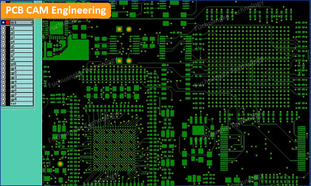
CAM Engineering Process
The Gerber files sent with each order are standardized so that they can be processed through PCB panelization step as well as through our PCB board manufacturing processes.
Basic Steps of Normalization Process:
- Re-naming the Gerber files to our standard naming convention.
- Checking to ensure that all necessary files are present.
- Importing Gerber and NC drill files into our CAM software.
- Reviewing that the PCB board’s specifications in the order match the data supplied.
- Checking the specs of these Gerber files with our manufacturing capabilities
Check to see our full PCB manufacturing capacities:
FPC and Rigid-Flex PCB Capabilities
Outer Layers Check
- Pads are removed for NPTHs, unless pads are much bigger than hole size.
- Test Outside of outline is removed, or move to inside of outline.
- The board outline is removed from artwork if present.
- Pads are added for all holes that do not have pads for standard specifications as all holes are plated.
- Copper extensions for gold fingers will be added to connect to gold bus bar.
Inner Layers Check
- 20mil clearance border will be added around negative inner layers for the outer edge. Clearances will be increased to 20mil (each side 10mil) over the hole size when possible around a drill hole and around the edge of a cutout. If all of these cannot be done without impacting the connectivity of the planes the order will be placed on hold. This is done to accommodate the inner layer clearance requirement at least 10mil from the edge of a hole to any adjacent copper on inner layers, and to prevent exposed copper.
- Clearances that are smaller than the hole size are assumed to be intended as direct connections to the plane and will be removed.
- On boards with edge fingers that will be beveled a 150mil clearance will be added along the edge that will be beveled. This is required to avoid exposed copper along the beveled edge.
- Text outside of outline is removed.
- The board outline is removed from positive artwork if present.
Drill Files
- NPTH holes are identified and labeled.
- Drill files are saved in a standard format.
- Double drill hits (duplicate drills), and any drill hits with smaller drill hits inside them will be removed.
- Drill chart tolerances that are all blank, or +/-0 will be ignored and the order type tolerances will be used instead.
Rout Files
- CNC files can not be used for extracting data.
- PCB board outlines on .GKO (Gerber Keep-out, outline) layers will need to be verified as the actual outline.
- The largest diameter routing is 93mil (2.4mm) (used to produce 100mil spacing), using this bit reduces routing costs by allowing multiple panels to be simultaneously routed but will increase the PCB price in mass PCB board production.
- The cutting path that the machine takes is called the NC route path; normally you need not to worry about it. You want to relay to manufacturing any specific cutting requirements you might have.
- With regard to the PCB board and slot outlines. We would prefer to have these included in the Gerber files (solder mask and drill/fab files) with a line width 5mil or 10mil. This line width will not affect the PCB board price as the PCB board outlines are disregarded when the minimum trace width is determined.
Solder Mask
- Clearances are increased to meet the minimum of 4mil swell for manufacturing. This is 2mil per a side. If clearances will expose traces or ground plane an FYI will be sent and we will continue to process the order as is. If soldermask clearances are missing then the order will be placed on hold for verification.
- Text outside of outline is removed.
- The PCB board outline will be added to this layer if not already present. This will be used for reference during production.
Basic Vias Protection Fuchuangke Technology Supports
Exposed Vias
- These will be processed with a clearance in the solder mask image that is equal to or greater than the via pad size plus 5mil solder mask swell.
- If you have a requirement other than this, we can accommodate clearances as small as the finished hole size plus 5mil. Please include any specific requirement in the fabrication notes and/or order documentation.
- These can be quoted and ordered with our standard parameters.
- Unless prior arrangements have been made, PCB boards will be built based on the solder mask image files submitted.
- Most design software packages have accommodation for including or excluding the vias from the solder mask image.
Tented Vias
- These will be processed with no clearance in the solder mask image for the vias.
- This will result in the pads being covered with solder mask and the holes may be open, partially plugged or completely plugged.
- As we do not have dry film solder mask available, we cannot offer vias tented in such a way as to guarantee that all of the holes will be completely covered.
- These can be quoted and ordered with our standard parameters. Unless prior arrangements have been made, the board will be built based on the solder mask image files submitted.
- Most design software packages have accommodations for including or excluding the vias from the solder mask images.
Plugged Vias
- These will be processed with an additional process that will fill the vias with a solid material that will prevent solder and air flow through the vias.
- The entire via cavity may not be completely filled.
- These orders will require a custom quote.
Filled Vias
- These will be processed with an additional process that will fill that vias a solid material that will prevent solder and air flow though the vias.
- The entire via cavity will be filled.
- These orders will require a custom quote.
Silkscreen Check
- We increase any text widths below 5mil to a minimum of 5mil.
- A silkscreen clip layer (corresponding solder mask layer) is created to eliminate ink on pads. We do not add via clearance if the vias are tented.
- The board outline is removed from artwork if present.
- Text outside of outline is removed.
Solder Paste Check
- We delete outside text and panelized if design is ordered as an array.
Additional Markings Check
- UL logo, date code (WWYY or YYWW), RoHS, 94V-0 and others may require, will be added in either a copper layer or a silkscreen layer unless otherwise specified. An internal reference number will be added in a copper layer but need to get your approval.
- Additional customer required markings will be added as requested.
Panelization Arrays: Scoring, V-Grooving, V-cut | Tab-Routing
What Is Scoring (V-cut)?
Scoring is a V-cut into the top and bottom surfaces of an array configuration of multiple PCB’s or a PCB with removable rails or frame. The cut depth is set such that the material left is the lesser of 1/3 of the finished thickness. When this process is used, the PCB boards are typically set up by side and end to end with no gap between the edges. This results in the V-cut into the area of the PCB boards, so a 150mil clearance between the edge of the boards and any conductors is required.
V-cut Panelization Array for You
- Single PCB board files provided by you.
- The total number of PCB board in the array and if the number of PCB board in the X direction and the Y direction.
- The width of the top, bottom, left and right rails if required.
- Indicate your required V-cut array in fab drawing or email text or in illustration.
What’s Tab Routing?
A tab route is used to build arrays, often called “route and retain”. The customer can place more than one board (Same or different design) up in a given area in an array or panelized configuration. This is typically for the convenience of the customer or for PCB board assembly requirements that utilize pick and place machines to assemble components. The PCB boards are then separated by breaking or cutting the tabs. Tabs are usually 100mil in width and are placed with at least 1 on each side of the boards.
Tab Rout PCB Array for You
- Your single PCB board files.
- The total number of PCB board in the array and if the number of PCB board in the X direction and the Y direction.
- The width of the top, bottom, left and right rails if required.
- Indicate your required tab-routing array in fab drawing or email text or in illustration.
PCB Panelization Process
During the PCB panelization process, the Gerber files prepared during the normalization process are copied to fill our big PCB production panels. Here are the basic Panelization Process
- Importing Gerber and NC drill files into our CAM software.
- Step and repeating the patterns into the usable area of our production panels.
- Adding the panel identification and tolling features to the border of the panels.
- Saving Gerber patterns of the panel artwork (copper layers, solder mask layers and legend layers and etc.), and forward them for building laser photo plot.
- Saving NC drill files and placing them on our network so that they will be available for the CNC controllers to retrieve.
- Creating the NC rout programs that are used to add slots, large holes and cut the individual PCB boards from the production panels. These are then placed on our network so that they will be available for the CNC controller to retrieve.
- Preparing the data files used for our Quality Assurance steps. The reference data that is used for Automation Optical Inspection (APQI) and Electrical Test (E-test) are prepared and placed on out network so that they will be available when needed during PCB board production.
Quick Quote
Any demand of PCB manufacturing or PCB assembly related to FR4 PCB, FPC, Rigid-Flex Board and IMS PCB, click below button to get quick quote. More questions, just contact our sales team.
FR-4 PCB Quote Flexible PCB Quote Rigid-Flex PCB Quote IMS PCB Quote