PCB assembly starts from solder paste printing with a SMT Stencil uploaded to an automated solder paste printer. The volume of solder paste (Tin) printed onto the SMT pads of the bare printed circuit boards is controlled by the thickness and aperture (windows) dimensions of the SMT Stencil. Using a good quality SMT stencil is a good start to build high quality PCB Assemblies.
Most of work of designing a Solder Paste Stencil is done in the PCB layout software that you use. The Stencils are designed based on the size, shape, and position of the pads of the various surface-mount components in the design layout. A Stencil can be no more accurate than the patterns (footprints) of the parts in the design.
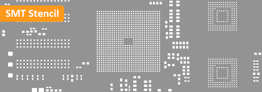
Framed SMT Stencil contains stainless steel sheet, Aluminum frame and glue between the sheet and frame. The apertures of the Solder Paste Stencil are cut by laser, and the information, like PCBA part number and stencil manufacturing date are also marked by laser on the sheet or the frame. Generally, Framed SMT Stencils with smooth aperture walls are designed and made for low to high volume screen printing on bare PCB boards, and which are applicable for 16mil pitch and below for micro BGA assembly. The exact procedure for generating a Gerber file for the paste layer (GTP and/or GBP) depends upon the software you are using, But the general process is the same in every software. The drawing below is from GTP layer (Solder Paste Stencil) from a 6-layer Rigid-flex PCB for UAV application. This GTP layer need to be modified before making the Solder Paste Stencil.
With our Turnkey PCB and Assembly Service, we will provide Framed SMT Stencil for your PCB assembly project. After checking the actual SMT pads and components land density, our experienced SMT engineer knows how to control the laser aperture dimensions, stencil thickness and size, and whether need to make GTP and GBP on one Stencil. Making a Laser Stencil suitable for your bare PCB panel and the Solder Paste Printer is cost saving and will improve the SMT quality and efficiency. All SMT Stencils upon the PCB Assembly order will be made till the bare PCB board arrival, and the SMT Turnaround is 1 working day. In the Stencil manufacturing process, the sheet and apertures will go through electroplating, then we can get smooth, polishing and clean SMT Stencil appearance.
| Framed SMT Stencil Specifications | |
| Technology | 100% laser cut |
| Material Used | Stainless Steel, Aluminum (frame) |
| Frame Types | Cast, Space Saver |
| Stencil Thickness | 0.10mm, 0.12mm, 0.15mm, 0.2mm |
| Minimum Cut Width | 0.50mm |
| Maximum Size | 500x500mm |
| Aperture Tolerance | within 6.35µm (0.25mil) |
All SMT stencil design should be as per IPC-7525A. Click to view our PCB blog to know details:
How To Understand IPC-7525A Stencil Design Guidelines
Besides, we also provide frameless SMT stencils and BGA Assembly stencils for customers who want to hand soldering components to their simple PCB Prototype Assembly.