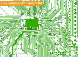
Common PCB Assembly Faults and Prevention
One of our main PCB assembly aims at Fuchuangke Technology is to take actions to minimize and prevent all common PCB assembly faults. This is one of the many ways that we ensure the highest quality possible for your projects. Due to the varying complexity for each PCB design, we understand that there are opportunities for PCB failure issues to arise if proper care is not taken beforehand. We understand the PCB fabrication process and using our knowledge and consideration, we take a variety of steps in order to prevent these issues. Many of these common issues are listed in following paragraphs.
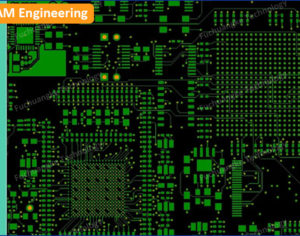
DFM Checks
We offer free DFM checks in order to help reduce the risk of common PCB assembly faults occurring. Its purpose is to assist our customer in the design stage of their circuit boards so that they can be manufactured quickly and efficiently. Our DFM guidelines define the various tolerances, and testing procedures to which we adhere during PCB fabrication.
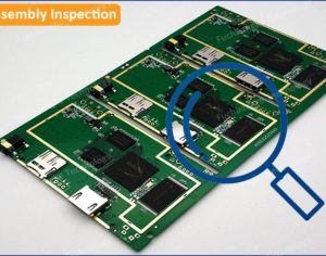
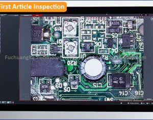
X-ray Inspection
We perform X-ray inspection of leadless parts such as BGA components, to ensure that proper solderability is attained. X-ray inspection machine exhibit grayscale drawing, which show variations in the form and thickness of a part. High-density features create a darker picture as compared to lesser density or thickness. As a result, it enables to quantitatively calculate these features and form association between suitable or unwanted manufacturing methods. Our qualified team uses X-ray inspection to resolve the majority of the problems. X-ray inspection is done in real time to continuously verify the quality steps followed. It assists us to examine the solder joints which are difficult to check via conventional methods. It also supports in validating oven profiles.
Via in Pad
Consider, if in your PCB design there are vias on or touching certain pads, also known as “active pads”. When a via is designed within an SMT pad, there is a high risk of solder leakage through the pads during circuit board assembly. In order to combat this, a non-conductive epoxy is generally used, however, this comes at an extra cost. If the vias are small enough and few enough, it may be possible to just fill the holes with solder mask with no risk to your circuit boards.
Solder Bridges
A short may occur during PCB assembly if there is an insufficient solder mask between pins. Designing boards without properly distributing the weight of the components can also contribute t this. It is very important to design the pads to have enough space between them and the solder mask layer. Component alignment issues may also occur if a proper X-Y file is not implemented, as it is very important to the SMT assembly. For a detailed example on how to generate pick and place files on design tools.
Clearance
Insufficient copper to edge clearance, where traces too close to the edge of the board can cause damage to occur during routing. If the copper is too close to the edges, during trimming, part of the coating that protects the copper from corrosion and interacting with the environment can be trimmed as well. If this occurs the copper would then be exposed, and it would be possible for exposed copper planes to make contact with one another by touching a conductive metal at the same time (which would of course cause a short). A bystander will also have an increased possibility of receiving an electric shock. For this reason, it is very important that the minimum clearances for the specific type of circuit board that is being fabricated are adhered to.
Plating Voids
Insufficient copper plating on the inside walls of the plated-thru holes on the PCB. This can case the PCB boards to be defective as the electrical current will not be able to pass between the layers. We can avoid this by ensuring that the holes are thoroughly and properly cleaned after drilling. This helps to prevent any contamination of the material or air bubbles insider of it.
De-Wetting/Non-Wetting
De-wetting can occur when the molten solder paste does cover a lead or pad, but then retreats and leaves behind a mound of solder. Non-wetting occurs when the solder only partially covers a surface leaving some exposed copper behind. Both of these issues can be avoided by making sure the component parts are still within their usable shelf lives and the flux being used must not be past it’s prime (after long hours of use).