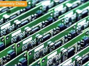
SMT PCB Assembly Manufacturing Service
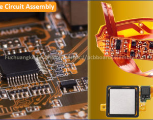
Turnkey PCB Assembly Service
| PCB Assembly | Surface Mount (SMT) & PTH Assembly with Single-sided & Double-sided Placement |
| Order Volume | 5~10k+ pcs (Single Pieces or Panelized PCB) |
| PCB Layer Count | 1-20 layers |
| PCB Type | Rigid, flexible & rigid-flex PCB Assembly |
| Components | Full Turnkey, Partial Turnkey & Consignment |
| SMT Stencil | Laser Cut Stainless Steel |
| Soldering Method | Only Lead-free Assembly |
| Lead Time | 2-3 working days |
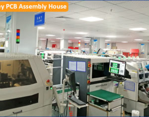
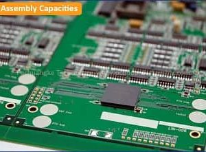
| Capabilities | SMT Equipment | PCB Assembly Capabilities |
What’s SMD Assembly Features?
- Dense SMD components assembly onto the bare printed circuit board
- Trends to double-sided PCB assembly from single-sided assembly
- Smaller SMD component package to 0201 and 01005
The higher density component in the SMD assembly allows for greater miniaturization of the circuit boards and assemblies, and which contributes to assembly project cost-down. Modern SMD placement machines provide faster SMD assembly speed, and the turnaround will be shorter for your PCB assembly manufacturer.
What’s SMT (Surface Mount Technology)?
As all we know, SMT assembly is the main technology of electronic assembly used to mount SMD components to the pad surface of the PCB board as oppose to inserting thru-hole components into plated thru-holes (PTHs) as with traditional PCB assembly service. SMT assembly was developed to reduce manufacturing costs, make more efficient occupation of PCB space, and also improve assembly work efficiency. As a result, surface mounting can build highly complex electronic circuit board into smaller and smaller assemblies with good repeatability due to the higher-level assembly automation.
What’s SMT Assembly Manufacturing Process?
The SMT PCB assembly process starts during the PCB layout stage when a lot of different electronic components are selected and the printed circuit board is designed by a design software like Altium Designer, OrCad, Allegro or PADS. It is vital to come true that the assembly process at this stage because this is the best time to incorporate as many features as possible that will make PCB assembly production straight forward. Quite often copper conductors are taken from the schematic design stage to PCB layout with the main considerations being the device functionality, which of course is very important, but design for manufacturability and assembly should ideally be incorporated.
Once the PCB design has been completed and components selected the next stage is to send the Gerber file and BOM (bill of materials) away to a turnkey PCB assembly manufacturer. The PCB Panel design should be considered upon how to improve SMT assembly efficiency, and PCB manufacturing specifications created including surface finish, copper clad laminate (CCL), finished copper weight and etc. to ensure that the format that the PCB boards are expected and suitable for the PCB manufacturing and assembly machines to be used.
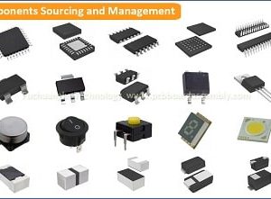
Electronic components that will soldered on the PCB board are available packaged types in many different ways such as on reels, tubes or trays. Meanwhile, for some big assembled modules, like Arduino devices, they are packaged in ESD ?electrostatic prevention?bag. But most components are available on reels which is preferred but sometimes due to MOQ (minimum order quantity) or small quantity demand, components are quite often supplied in tubes or in short strips of tape (known as cut-tapes) for PCB assembly prototypes. Both of these packaging types can be used on our SMT assembly machines, but do need appropriate feeder types. All components with an MSL (moisture sensitivity levels), like ICs, RAMs, NANDs, LEDs or others, should be handled in accordance to JEDEC J-STD-033B standards, the baking time should accord to components datasheet requirements.
SMT Stencil Design
When the bare printed circuit boards in single pieces or panel are prepared well, the PCB assembly manufacturer should check the pads window sizes, shapes, other values, BOM, and compare these pads with the original Gerber GTP (top paste) and GBP (bottom paste) files, then to decide the SMT stencil design and stencil thickness, which will ensure all windows on the stencil will be appropriate and suitable. And in this checking phrase, the engineer will remove the non-populated pad windows. Of course, stencil design and fabrication should be conformal with IPC-7525A guidelines.
For More Information: How To Understand IPC-7525A Stencil Design Guidelines
Machine Programming – Gerber to Centroid / Pick-and-Place / XY File
PCB assembly machine programming, also called setup, the time is not particular order between machines setup and SMT stencil design. If PCB boards and electronic components are ready on hand, the main step is to setup the various machines used with SMT assembly manufacturing process. Machines including solder paste inspection, placement machine and AOI will require a program to be created which is best generated from the Gerber files or CAD data. In programming process, it is mainly to create the centroid (coordinates) / placement (pick-and-place) / XY file can be read by the machines. The program engineer also needs to identify the polarities of some required components. If the PCB board assembly requires double-sided assembly, there will be two centroid / placement / XY files on top and bottom.
Solder Paste Printing
In the whole PCB assembly process, the first setup machine is solder paste printer, which is used to apply solder paste with a SMT stencil and squeezes to cover appropriate solder paste onto the PCB board pads required. The wettability and volume of solder paste, and the thickness and windows sizes of the stencil will decide whether there are assembly defects in afterwards reflow soldering process. Solder paste printing is a very important process, and that’s why we utilize MPM Elite printer made in USA. Keeping control of this process is critical as any printing defects as possible. With PCB assembly becoming more complex, the stencil design must take care to ensure a repeatable and stable process.
Solder Paste Inspection
Compared to solder paste printing, most people are not familiar with solder paste inspection (SPI) machine, which is designed to measure the volume, square, height, location, shape and alignment of the applied solder paste. If the pictures taken by the 2MP CCD camera are the same or within the tolerance compared to the acceptable sample picture. The printed PCB board will go through to the next placement machines. SPI inspection will prevent from solder paste printing defects, then to improve the high-volume PCB assembly production yield. Don’t ignore whether your turnkey PCB assembly supplier has a 3D SPI machine. If only rely on AOI to prevent assembly defects, sometimes, it’s late. If solder paste is spread out the pads, the components soldered need extra time to rework. What’s worse, in some assembly instances, some components or the pads will be broken during rework.
SMD Component Assembly (Pick-and-Place)
Once the PCB board has been confirmed to have the correct amount of solder paste applied, it moves into the next part of the PCB assembly manufacturing process which is SMD component assembly, always known as pick-and-place. Each component is picked from the component feeder using either a vacuum or gripper nozzle of the placement machine, checked by the high definition (HD) camera vision system and placed in the correct location according to the centroid / placement / XY file programmed at the very beginning at high speed with high precision. There is a lot of machines available in the market for this process, but at Fuchuangke Technology, we are equipped with Fuji and Panasonic highly stable placement machines in this process. Of course, which brand and machine a SMT assembly manufacturer should select? It depends on the business. Like us, we focus on low to high-volume PCB assembly, then the pick-and-place speed is very vital. What’s more, we also support PCB assembly prototype and small batch.
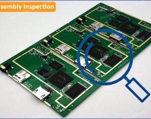
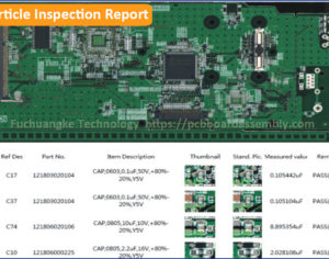
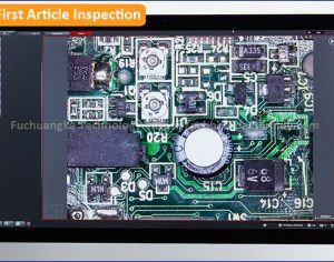
First Article Inspection (FAI)
One of the many assembly challenges for some SMT PCB assembly suppliers is the verification of the first PCB assembly to customer information or first article inspection (FAI) as can be very time consuming. If verified by the customer, the supplier has to stop machines and restart machines after the verification from the customer. The PCB assembly efficiency will be reduced, and in this stop period, the SMT supplier can not assemble other projects, so what need to do is to wait. But first article inspection is very important as any errors, if undetected, can lead to high volumes of rework. As a customer or an end-user, you must don’t want the electronic hardware are reworked. We conduct 100% first article inspection on all PCB assembly projects, and we can provide FAI report extracted from our FAI-600 system.
More information:
How Much Do You Know About PCBA First Article Inspection?
SMT First Article Inspection on PCB Board Assembly
Reflow Soldering
Once all component placements have been checked, the PCB assembly with solder paste adhered components moves into reflow soldering machine where all the electrical solder connections are formed between the components and the PCB board by heating the assembly artwork to sufficient temperature. The reflow soldering machines we utilize are Heller with 13 temperature control zones including 10 forced convection zones on both top and bottom, and 3 cooling zones. The correct reflow profile is key to ensure acceptable solder joints without damaging the electronic components or assembly due to excessive heat. For some components on uncommon thickness PCB boards, we will measure the temperature between the PCB pads and the bottom pads of the component to ensure no soldering defects. The accuracy of temperature controller is +/-0.1?, the cross-belt temperature tolerance is +/-2.0?. With so highly precision temperature control in reflow soldering process, we are capable of assembling your highly complex PCB boards with good quality. When using lead-free assembly, a carefully profiled assembly is even more important as the required reflow temperature can often be very close to many components maximum rated temperature.
Post-Reflow AOI
The last part of the SMT PCB assembly process is to check that no mistakes have been made by using an automated optical inspection (AOI) machine to check solder joint quality. Our VT-RNS AOI machine delivers outstanding performance at every step of production. Easy-to-set initial inspection parameters are ready for immediate use to perform high accuracy inspection. Data collected from the inspection stations can be analyzed for root cause analysis of defects for ongoing process improvement. AOI process will increase SMT PCB assembly productivity.
X-ray Inspection
For some components, especially for those BGA and QFN packages, solder joints are hidden and unvisitable on the bottom of the packages, technicians in SMT facility can not verify the solder joints by visual or AOI inspection. When a PCB assembly passed the AOI, it comes to X-ray machine to inspect the hidden solder joints quality. X-ray makes it possible to check underneath components, amount of voiding present within solder joints and also can be used to verify the solder hole fill after soldering process. The Phoenix x|aminer X-Ray machine we are using is an easy to use X-ray inspection system for components and PCBA with strong performance. If customer requires X-ray photos on their PCB assembly, we can provide for free.
Quick Quote
Click the Quick Quote buttons below, you can turn to the different PCB quote pages. Just fill in the PCB specifications, upload Gerber files, BOM, Assembly Drawing and Pick-and-Place file, you will get quick quote of PCB board and PCB Assembly.
FR-4 PCB Quote Flexible PCB Quote Rigid-Flex PCB Quote IMS PCB Quote