IEEE-1149 JTAG Boundary-Scan for PCB Assembly Testing
PCB Assembly Functional Testing (FCT)
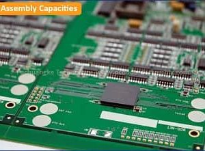
Fuchuangke Technology offers a comprehensive range of PCB assembly functional testing (FCT) services. FCT is conducted in the last step of PCB and assembly manufacturing process to determine the quality of the PCBA. It helps us detect various PCB assembly issues such as circuit open, short, incorrect part or orientation
From simple power checks, program uploading, JTAG and AOI through to calibration and product conformance all performed by skilled engineers in our PCB assembly testing and inspection procedure. For surface mounting device (SMD) assembly quality standards are maintained using the AOI machines and software to assist inspection where the human eye can not realize, ensuring that the right components are placed in the right orientation and in the right place. For testing and inspection, our first article inspection (FAI) can also measure the values of capacitors, resistors and inductors, allowing us to fine tune our assembly manufacturing processes, improve quality where needed, reduce rework and increase first time passes. Every batch is subjected to 100% AOI and FAI.
A team of qualified testing engineers provide functional testing for your PCB assembly (PCBA) and instrumentation calibration supported by advanced In-Circuit testing (ICT) when appropriate. We work with customers to develop testing and calibration strategies that to cover PCBA testing, environmental cycling, program uploading and every key measurement is recorded, electrically in a device history record, retained for the life of the product. When your printed circuit board assembly (PCBA) project comes to outsourcing manufacturing and functional testing, you want functional testing to be done with the same PCB assembly supplier but not by yourselves or one another supplier, then you can only contact with the turnkey PCB and assembly manufacturer, like Fuchuangke Technology.
Do You Know JTAG/Boundary-Scan?
Joint Test Action Group (JTAG) is the common name used for a debugging, programming, and testing interface typically found on microcontrollers, ASICs, and FPGAs. It enables all components with this interface to be tested, programmed, and/or debugged using a single connector on a printed circuit board (PCB) assembly which can daisy chain them together.
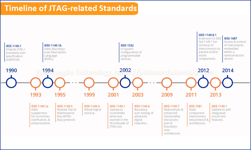
In 1990, the Institute of Electrical and Electronics Engineers (IEEE) codified the results of the effort of Joint Test Action Group (JTAG) in IEEE Standard 1149.1-1990, entitled Standard Test Access Port and Boundary-Scan Architecture. Then JTAG/Boundary-Scan has continuously grown in adoption, popularity, and usefulness – even today, new revisions and supplements to the IEEE-1149.1 standard are being developed and implemented.
What’s JTAG?
JTAG, commonly referred to as boundary-scan and defined by the institute of IEEE 1149.1, originally began as an integrated method for testing interconnects on printed circuit boards (PCBs) implemented at the integrated circuit (IC) level. As PCBs grew in complexity and density-a trend that continues today-limitations in the traditional test methods of in-circuit testers (ICTs) and bed of nails fixtures became evident. Packaging formats, specifically Ball Grid Array (BGA) and other fine pitch components, designed to meet ever-increasing physical space constrains, also led to a loss of physical access to signals.
These new technology developments led to dramatic increases in costs related to designing and building bed of nails fixtures; at the same time, circuit test coverage also suffered. JTAG/boundary-scan presented an elegant solution to this problem: build functionality into the IC to assist in testing assembled electronic systems. Today, JTAG is used for everything from testing interconnects and functionality on ICs to programming flash memory of systems deployed in the field and everything in-between. JTAG and its related standards have been and will continue to be extended to address additional challenges in electronic test and manufacturing, including test of 3D ICs and complex, hierarchical systems.
History of JTAG
In the 1980s, the Joint Test Actional Group (JTAG) set out to develop a specification for boundary-scan testing that was standardized in 1990s as the IEEE Standard 1149.1-1990. A few years later in 1993, a new revision to the standard-1149.1a-was introduced to clarify, correct, and enhance the original specification. An additional supplement, 1149.1b, was published in 1994 to add Boundary-Scan Description Language (BSDL) to the standard, paving the way for fast, automated test development and spurring continuous adoption by major electronics producers all over the world. The lessons that were learned became formalized in an update to the core standard in 2001 and IEEE01149.1-2001 was published.
As new applications of JTAG were discovered, new standards were developed to extend the capabilities of JTAG. Standards such as the IEEE-1149.5 modules test and maintenance bus standard in 1995 and the IEEE-1149.4 standard for mixed-signal testing in 1999 were met with low adoption rates and are not widely used at present. The IEEE-1149.6 standard introduced in 2003, on the other hand, began with slow adoption but has since become standard in many ICs as the technology it addressed-high-speed, AC-coupled signals-became a common feature of electronic systems. IEEE-1149.7, published in 2009 to address the need for JTAG in low-pin-count systems, is now standard on many popular microcontrollers.
Additional standards have also been published to add specific test capabilities. In 2002, the IEEE-1532 standard for in-system configuration of programmable devices was released and is now a common feature of FPGAs and their supporting software systems. IEEE-1581 was developed in 2011 to provide a convenient method of testing interconnects of high-speed memories with slow-speed test vectors; a version of this capability is implemented in some DDR4 memory components. To address the new application of combined capacitive sensing and boundary-scan test, IEEE-1149.8.1 was published in 2012. The extensibility of JTAG has been proven time and again.
More recently, efforts have been made to standardize JTAG access to instruments embedded with ICs. The IEEE-1149.1 standard was updated once more in 2013 for some housekeeping and to add extensions to access these instruments. Just one year later, an alternative standard for accessing these instruments, IEEE-1687, was published. Looking to the future, industry activities to extend JTAG into 3D-IC testing, system-level testing, and high-speed testing are already underway, proving that the versatility and extensibility of JTAG is here to stay.
HOW JTAG Works?
The JTAG/boundary-scan test architecture was originally developed as method to test interconnects between ICs mounted on a PCB without using physical test probes. Boundary-scan cells created using multiplexer and latch circuits are attached to each pin on the device. These cells, embedded in the device, can capture data from pin or core logic signals as well as force data onto pins. Captured data is serially shifted out through the JTAG Test Access Port (TAP) and can be compared to expected values to determine a pass or fail result. Forced test data is serially shifted into the boundary-scan cells. All of this is controlled from a serial data path called the scan path or scan chain.
Because each pin can be individually controlled, boundary-scan eliminates a large number of test vectors that would normally need to properly initialize sequential logic. Using JTAG, tens of hundreds of test vectors my do the job that has previously required thousands. Boundary-scan enables shorter test times, higher test coverage, increased diagnostic capability, and lower capital equipment cost.
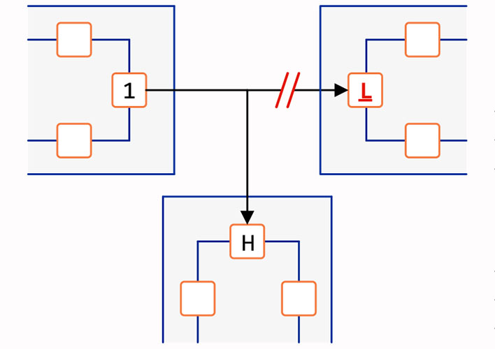
The principles of interconnect test using boundary-scan components are showed in below figure. Two boundary-scan compliant devices are connected with four nets. The first device includes four outputs that are driving the four inputs of the other with predefined values. In this case, we assume that the circuit includes two faults: a short between Net2 and Net3, and an open fault on Net4. We will also assume that a short between two nets behaves as a wired-AND and an open fault behaves as a stuck-at-1 condition.
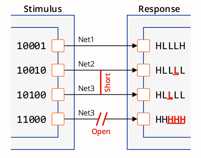
To detect and isolate defects, the tester shifts the patterns to the inputs of the second device. The input values and applies these patterns to the inputs register of the second device are shifted out and compared to the expected values. In this case, the results, underlined and marked in red on Net2, Net3, and Net4, do not match the expected values and the tester tags these nets as faulty. Sophisticated algorithms are used to automatically generate the minimal set of test vectors to detect, isolate, and diagnose faults to specific nets, devices, and pins.
Of course, interconnect testing is just one of may uses of JTAG-the aforementioned JTAD TAP has been extended to support additional capabilities including in-system-programming (ISP), in-circuit-emulation (ICE), embedded functional testing, and many more. The standard accounts for the addition of device-specific instructions and registers that can be used do interact with additional IC capabilities. For example, a microprocessor device may have embedded functionality for data download, program execution, or register peek-and-poke activities accessible using JTAG TAP; using the same tools, FPGA and CPLD devices can be erased, configured, read-back, and controlled using JTAG instructions through the IEEE-1532 standard. More recently, embedded IC instrumentation-from instruments that measure voltage and current to devices that can execute high-speed test on the chip-has used the JTAG TAP as the access mechanism, providing new visibility into the IC and further expanding the scope of JTAG testing.
Product Life-Cycle Phases and Applications
While JTAG/boundary -scan was originally regarded as a method to test electronic products during the production phase, new developments and applications of the IEEE-1149.1 standard have enabled the use of JTAG in many other products life cycle phases. Boundary-scan technology is commonly applied to product design, prototype debugging, and field service.
The same test suite used to validate design testability can adapted and utilized for PCB board bring-up, high-volume manufacturing test, troubleshooting and repairs, and even field service and reprogramming. The versatility of JTAG/boundary-scan tools delivers immense value to organizations beyond the production phase.

JTAG Test Overview
While originally developed to address the needs of testing printed circuit board assembly (PCBA) interconnects, JTAG test methods can be used to address many needs beyond simple structural test. This overview briefly examines popular types of JTAG tests and applications.
JTAG Test Basics
Most JTAG/boundary-scan systems are composed of two main components: a test program generator for test development and creation, and a test program executive for running tests and reporting results.
Test Program Generator
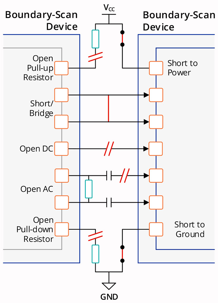
Test program generators accepts computer aided design (CAD) data as input in the form of netlist, bill of materials, schematic, and layout information. The test program generator (TPG) uses the information provided in these files, along with guidance from the test developer, to automatically create test patterns for fault detection and isolation using JTAG-testable nets on the PCB. Full featured test program generation software will generally also include the capability to automatically generate tests from non-scannable components including logic clusters and memories that are connected to boundary-scan devices. A sample of faults that can be detected with automatically generated tests is shown as below figure.
Test Program Executive
Test program executives are used to run the tests created by the test program generation software. The test executive interfaces with the JTAG hardware to execute test patterns on a unit under test (UUT), then compares the results with expected values and attempts to diagnose any failures. Modern test executives include advanced features such as flow control, support for third party test types, and often include an application programming interface (API) for integration with additional test systems or development of simplified operator interfaces.
JTAG Benefits
The continuous drive toward higher density interconnects and finer pitch ball-grid-array (BGA) components has fueled the need for test strategies that minimize the number of test points required. By embedding the test logic within the IC itself and limiting the physical interface to just a few signals, JTAG/boundary-scan presents an elegant solution to testing, debugging, and diagnosing modern electronic systems.
Today, JTAG provides the access mechanism for a variety of different system operations. Just some of the benefits provided by JTAG are:
- Result through the product life cycle. The simple mechanism provided by the JTAG TAP can be used at all stages of the product lifecycle-from benchtop prototype debugging to high volume manufacturing and even in the field.
- Test point reduction. JTAG provides test access through just 4 pins (2 pins for IEEE-1149.7 compliant devices), reducing the number of test points required, resulting in lower PCB fabrication costs and reduced test fixture complexity.
- Independent observation and control. Boundary-scan tests operate independently of the system logic, meaning they can be used to diagnose systems that may not operate functionally.
- Extensibility. JTAG has seen continuous development and new applications are frequently being discovered. Additional standards have been developed to address AC-coupled testing, reduced pin counts, and control of test instruments embedded within ICs.
Scan Chain Infrastructure Test
JTAG testing usually begins by checking the underlying infrastructure to ensure that all devices are connected and test capabilities are operational. Test patterns are used to exercise the instruction register and boundary-scan register for comparison against expected lengths and values. If present, device ID codes can also be read and compared against expected values to ensure that the correct component has been placed.
Interconnect, Bus Wire, and Resistor Tests
After verifying that the scan chain is working properly, test patterns can be used to verify interconnectivity between system components. Nets that involve three or more boundary-scan pins represent a specific case, called a bus wire, where additional patterns can be used to isolate faults to a specific pin, as shown in below figure. During a buswire test, boundary-scan driver pins are tested one at a time to ensure that all possible opens are tested.
Devices that are transparent to DC signals can be modeled as “short” signal paths and included in the test; for example, series resistors can be tested for component presence and open faults, while directional buffers can be constrained and tested to ensure that signals sampled at the buffer output pins match the signals that are applied to the buffer input pins. Additionally, tests for AC-coupled signals can be integrated with interconnect and buswire tests in systems with IEEE-1149.6 standard components, allowing capacitors to be tested for AC signal transparency.
Special tests can also be used to check pull-up and pull-down resistors, ensuring that resistors are present in the assembled system in addition to testing the nets for open and short faults. To accomplish this, resistors are tested by first driving the signal to a state opposite the pulled value. The net is then tri-stated, allowing the resistor to pull the signal back to the original state. Finally, the signal is sampled and the value is compared to the expected pulled value.
Logic, Memory & Complex Devices
Not only can interconnect between boundary-scan components and simple transparent components be tested, but additional non-boundary-scan components can be controlled and tested for functionality and continuity using connected boundary-scan components. Simple test patterns may be used to test logic devices such as decoders or multiplexers, while sophisticated scripts may be used control and test complex devices for basic or advanced functionality, including analog-to-digital converters, UARTs, and Ethernet PHYs.
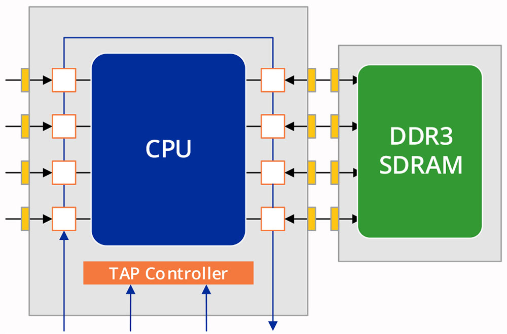
A common application of a cluster tests uses the storage capability of RAM devices to verify interconnects between a boundary-scan device and a connected memory, as shown in below figure. Using a model of memory component, tests can be automatically created to write specific data patterns to memory addresses and then read back and compared against to ensure that all memory data and address signals are driven to both high and low logic states. The same concept used to test RAM can also be applied to non-volatile memory, such as flash, EEPROM, and NVRAM components.
JTAG Embedded Test
Many modern processors use JTAG as the main interface for on-chip debugging (OCD), allowing the processor to be controlled over the JTAG port within an embedded system. Using this same interface, the JTAG port can be used to initialize a processor, download and run a test program, and then obtain results; this test technique is a fast, convenient method for developing and executing peripheral tests and in-system-programming operations in embedded systems. Because these tests run at the system processor speed, defects that may not be identified during low-speed execution can be detected.
In-System-Programming
In additional to test applications, JTAG is also frequently used as the primary method to program devices such as flash memory and CPLDs. To program flash devices, the pins of a connected boundary-scan-compatible component can be used to control the memory and erase, program, and verify the component using the boundary-scan chain. FPGC and CPLD devices that support IEEE-1532 standard instructions can be accessed and programmed directly using the JTAG port.
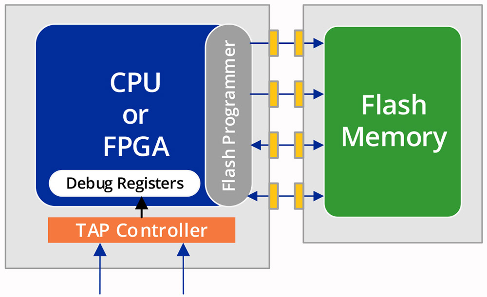
Faster performance can be achieved using a CPU or FPGA to program the flash. In these cases, a small flash programming application is downloaded to the controlling device over the JTAG port, which is then used to interface between the test system and the flash programming application running on the embedded system. This configuration Is depicted in below figure. This embedded JTAG programmer can run at much higher speeds than boundary-scan, increasing production throughput and rivaling or surpassing the speeds of USB and Ethernet-based programming solutions, without requiring an operating system or high-level software be present on the embedded system.
The IEEE-1149.1 JTAG team had the foresight to design an extensible standard-one that could employ additional data register for many different applications. As a result, JTAG has grown from its original roots for PCB board testing into a ubiquitous port that can be used for diverse applications such as in-system-programming, on-chip debugging, and more recently control of instruments embedded within ICs.
JTAG Chip Architecture
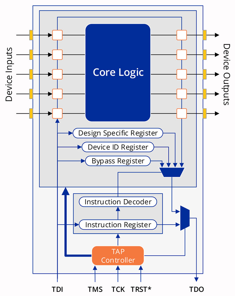
The IEEE-1149.1 JTAG standard defines how IC scan logic must behave to achieve interoperability among components, systems, and test tools. ICs consist of logic cells, or boundary-scan cells, between the system logic and the signal pins or balls that connect the IC to the PCB. Each cell provides specific test capabilities-some cells can be used as input, others as output, and some are bidirectional.
The boundary-scan cells within a device are connected together to form a shift register, which is accessed through a serial test data input (TDI) and test data output (TDO) interface. The Test optional reset signal, is the primary interface to the test controller which provides access to the logic.
JTAG Instructions
IEEE-1149.1 specifies mandatory instructions-to be fully JTAG compliant, devices must utilize these instructions.
EXTEST
The EXTEST instruction is used to perform interconnect testing. When the EXTEST instruction is used, the mandatory boundary-scan register is connected between TDI and TDO and the device is placed in an “external” test mode. In this mode, boundary-scan output cells will drive test data onto the device pins and input cells will capture data from device pins-this is the main instruction used for boundary-scan testing.
SAMPLE/PRELOAD
The SAMPLE/PRELOAD instruction is similar to EXTEST, but allows the boundary-scan device to remain in mission/functional mode while still connecting the boundary-scan register to TDI and TDO. When the SAMPLE/PRELOAD instruction is used, the boundary-scan register is accessible through data scans while the device remains functional. This is also useful for preloading data into the boundary-scan register without interrupting the device’s functional behavior, prior to executing the EXTEST instruction.
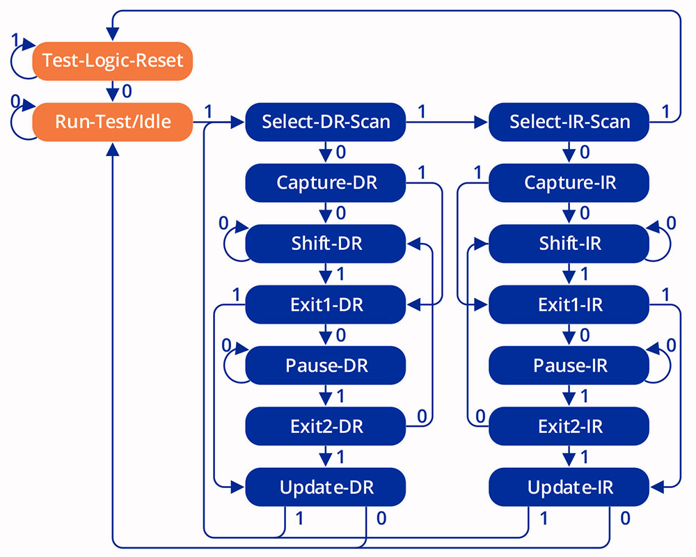
TAP Controller
The TAP controller as defined by the IEEE-1149.1 standard uses a 16-state finite state machine controlled by a test clock (TCK) and test mode select (TMS) signals. Transitions are determined by the state of TMS on the rising edge of TCK.
Two analogous paths through the state machine are used to capture and/or update data by scanning through the instruction register (IR) or through a data register (DR). The JTAG state machine is depicted in below figure.
JTAG Interface
The physical JTAG interface, or test access port (TAP) consists of mandatory signals and one optional asynchronous reset signal. Table below summarizes the HTAG TAP signals.
| Abbreviation | Signal | Description |
| TCK | Test Clock | Synchronizes the internal state machine operations. |
| TMS | Test Mode Select | Sampled at the rising edge of TCK to determine the next state. |
| TDI | Test Data In | Represents the data shifted into the device’s test or programming logic. It is sampled at the rising of TCK when the internal state machine is in the correct state. |
| TDO | Test Data Out | Represents the data shifted out of the device’s test or programming logic and is valid on the falling edge of TCK when the internal state machine is in the correct state. |
| TRST | Test Reset | An optional pin which, when available, can reset the TAP controller’s state machine. |
Many TAP interfaces will employ signals in addition to those required by the JTAG standard. For example, on-chip debugging applications may include signals for asynchronous halt and reset, while in-system-programming applications may increase programming speed by taking advantage of additional pins for time-critical function such as toggling the write enable signal or polling a ready/busy signal.
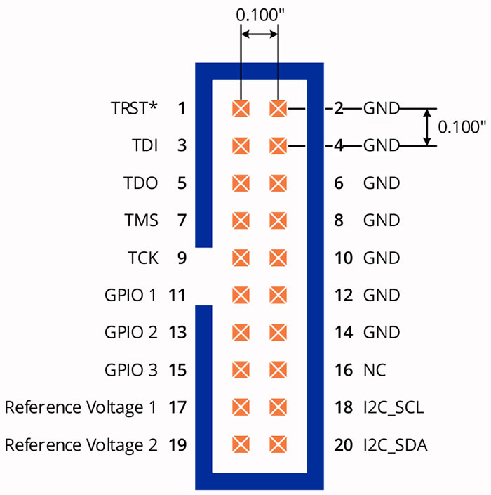
JTAG Connectors
There is no single standard JTAG interface connector or JTAG pinout-physical characteristics such as pin spacing, interface voltage, and pin order vary among devices. Some TAP implementations may include additional signals such as reference voltage, general purpose input/output (GPIO), or even serial bus signals, such as the example shown in below figure.
BSDL Files
Boundary-Scan Description Language (BSDL) files are used to describe the boundary-scan behavior and capabilities of a given device. Originally designed as a subset of VHDL, the BSDL format has been extended to add additional features and is not strictly VHDL compliant. The BSDL describes important properties of a given device’s boundary-scan functions, including:
- Which JTAG standard are supported by the device.
- Signal mapping and package information.
- Available instructions, and which registers those instructions access.
- The type of boundary-scan cell available for each signal.
- Information about signals that affect compliance to the standard.
- Design warnings and notes.
Over time, the BSDL format has also been extended to include additional information; BSDL files may include descriptions of AC (IEEE-1149.6) testing capabilities, sequences in procedural description language (PDL) format, information about an electronic chip identifier (ECID), and more. BSDLs include statements that specify which standards are supported to allow automated tools to utilize supported features.
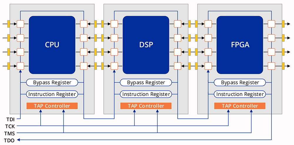
Scan Chain
JTAG devices may be daisy-chained within a system and controlled simultaneously. Boundary-scan test software can utilize one component to drive signals that will be sensed on a second component, verifying continuity from pin-to-pin. Devices can be placed in BYPASS mode to shorten the overall length of the chain to reduce test time. More complex designs may utilize additional circuitry or a dedicated JTAG bridge to selectively configures a scan chain that contains multiple devices, or even multiple sub-assemblies.
JTAG Applications
While it is obvious that JTAG based testing can be used in the production phase of a product, new developments and applications of the IEEE-1149.1 standard have enabled the use of JTAG in many other product life cycle phases. Specifically, JTAG technology is now applied to product design, prototype debugging and field service as depicted in figure below. This means the cost of the JTAG tools can be amortized over the entire product life cycle, not just the production phase.
To facilitate this product life cycle concept, JTAG tool vendors offer an integrated family of software and hardware solutions for all phases of a product’s life-cycle. All of these products are compatible with each other, thus protecting the user’s investment.
Applying JTAG for Product Development
The ongoing marketing drive for reduced product size, such as portable phones and digital cameras, higher functional integration, faster clock rates, and shorter product life-cycle with dramatically faster time-to-market ahs created new technology trends. These trends include increased device complexity, fine pitch components, such as surface-mount-technology (SMT), systems-in-package (SIPs), multi-chip modules (MCMs), ball-grid arrays (BGAs), increased IC pin-count, and smaller PCB traces. These technology advances, in turn, create problems in PCB development:
- Many PCB boards include components that are assembled on both sides of the board. Most of the through-holes and traces are buried and inaccessible.
- Loss of physical access to fine pitch components, such as SMTs and BGAs, makes it difficult to probe the pins and distinguish between manufacturing and design problems.
- Often a prototype PCB assembly is hurriedly built by a small supplier with lower quality control as compared to a mass production PCB assembly house. A prototype generally will include more assembly defects than a production unit.
- When the prototype arrives, a test fixture for the ICT is not available and, therefore, manufacturing defects cannot be easily detected and isolated.
- Small-size products Programmable Logic Devices (CPLDs) and flash memory devices (in BGA packages) are not socketed and are soldered directly to the PCB board.
- Every time a new processor or a different flash device is selected, the engineer has to learn from scratch how to program the flash memory.
- When a design includes CPLDs from different vendors, the engineer must use different in-circuit programmers to program the CPLDs.
JTAG technology is the only cost-effective solution that can deal with above problems. In recent years, the number of devices that include JTAG has grown dramatically. Almost every new microprocessor that is being introduced includes JTAG circuitry for testing and in-circuit emulation. Most of the CPLD and field programmable array (FPGA) manufacturers, such as Altera, Lattice and Xilinx, to mention a few, have incorporated JTAG logic into their components, including additional circuitry that uses the JTAG four-wire interface to program their devices in-system.
As acceptance of JTAG as the main technology for interconnect testing and in-system programming (ISP) has increased, the various JTAG test and ISP tools have matured as well. The increased number of JTAG components and mature JTAG tools, as well as other factors that will be described later, provide engineers with the following benefits:
- Easy to implement Design-For-Testability (DFT) rules. A list of basic DFT rules is provided later in this article.
- Design analysis prior to PCB layout to improve testability.
- Packaging problems are found prior to PCB layout.
- Little need for test points.
- No need for test fixtures.
- More control over the test process.
- Quick diagnosis (with high resolution) of interconnection problems without writing any functional test code.
- Program code in flash devices.
- Design configuration data placement into CPLDs.
- JTAG emulation and source-level debugging.
As a turnkey PCB and assembly manufacturer, Fuchuangke Technology is capable of conduct PCB assembly testing task if in need from customers.
Quick Quote
FR-4 PCB Quote Flexible PCB Quote Rigid-Flex PCB Quote IMS PCB Quote