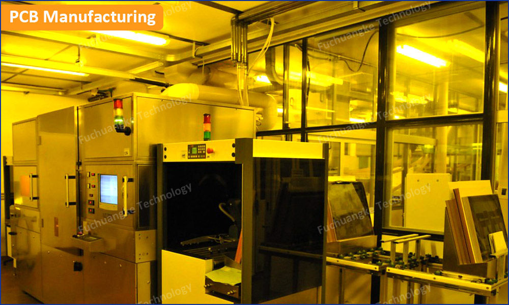
What Is Printed Circuit Board (PCB) Manufacturing?
Printed Circuit Boards (PCBs) can be seen in almost all electronic devices nowadays. Have you ever wondered what’s a printed circuit board manufacturing? PCB boards are typically made with copper on dielectric substrate material. Depending on the requirements, the copper is electroless plated and electric plated to a substrate and carved always to expose the pattern of the board. But there are multiple layers, the copper layers and dielectric layers must be lined up and bonded together for form a PCB board.
From this PCB blog, you will get some necessary knowledges about PCB Manufacturing, including PCB Manufacturing Basics, 16 PCB Manufacturing Processes for Standard FR4 PCB, and PCB Reliability Testing to know what PCB manufacturing is.
PCB Manufacturing Basics
- What is Stack-up?
Before knowing how to manufacture a printed circuit board, the first thing to know is stack-up, which can be simply understood as the copper layer quantity. Single-sided, double-sided, or many. If someone says a 6-layer PCB, you should first think it is a multilayer PCB with 6 copper layers. And each copper layer consists of many conductive copper patterns (traces), the wiring to support electrical connection between electronic components. How are these copper patterns connected between different layers? They are connected through plated-thru holes (PTHs).
But a real PCB is much more complex than this kind understanding. In-between the copper layers, there are dielectric layers to support insulation between conductive copper layers. And the structure of the copper layers and dielectric layers consists the PCB Stack-up. If provide you a stack-up, you will get some information, including layer count, copper thickness, core and PP thicknesses, board thickness and some others may contain.
- What is a PCB Fabrication (Fab) Panel?
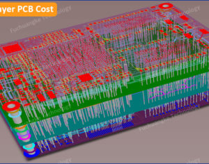
Maybe you’ve seen a lot of circuit boards with different size and shapes, but no matter how different they are, they are manufactured by making a large array of boards in a single sheet, which is called PCB Fabrication Panel, or Fab Panel. Even if your circuit board is small as a coin, it will begin production on a sheet of copper clad lamination (CCL) base material, usually 18’’x24’’, and your design will be replicated across base material until find the maximum usage rate, then to produce as many boards as possible from it. If you understand the PCB fabrication panel, it will be helpful for you to understand the volume PCB cost, your PCB unit price is based on the number of panels being produced, not the number of individual pieces you want to order.
Check to know more 8 Factors That Affect Multilayer PCB Cost
The PCB fabrication panel is different from the “panel” people always used to panelize their own design(s). This “Panel” in most people’s mind is always the glossary “Set” in PCB manufacturing industry, and PCB fabrication panel consists of many Sets. Until the very last step when individual boards or Sets are cut out of the fab panel, all PCB manufacturing deals with PCBs in that large, fab panel format.
- Front-end Engineering (Process Card & Planning)
When PCB manufacturer gets an order from the customer, the first step is to review the PCB designs, always Gerber files, and prepare them for PCB fabrication. In this step, the engineer may issue some engineering questions (EQs) before production for the customer to reply. This is mainly for better quality control and solve some design issues. Then a planer will create a set of step-by-step instructions, called as a “process card” to build the PCB. The process card will follow along with the work as it’s being completed.
To begin the manufacturing process, each set of design data and associated characteristics is assigned a unique fabrication number. In the future, if a customer re-orders the exact same design and makes any change, even as insignificant as the solder mask color of the PCB, a new fab number is assigned. This helps ensure proper tracking, as some customers re-use the same part number even as revisions are made. Like changing Rev 1 to Rev 2.
The process card contains information such as the manufacturing steps involved to build the PCB board, the quantity due, and the date due. To do this well, the planner is required to review all information related to the project including any production order details, fabrication drawings, and special instructions. Upon this information the certain department will ensure the proper materials are available for the project and will build the process card to reflect the production process required.
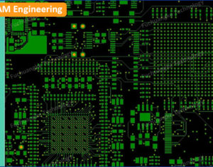
- CAM Engineering (EQs & Working Gerber Files)
When planning is complete, the next turn is the CAM engineer to perform an in-depth data review and create the tooling required to manufacture the PCB board. CAM engineers follow a detailed checklist for each project, and here are the key responsibilities.
Data Clean-Up: The CAM engineer will load the data into the CAM software and perform basic data clean-up, including checking file names and assignments and alignment of the layers. This is necessary because although data is provided in a standard format, like Gerber, or ODB++, each PCB design software package may output data a bit differently.
Drill / Rout Data Verification & Edits: The CAM engineer will verify that the hole size and counts from the data file match what is specified in the fabrication drawing. It should be noted that not every designer provides a fabrication drawing. While preferred, this is by no means a show stopper. They also check for any special routing or cutouts, as well as plated vs. non-plated holes. Depending on the requirements, there could be multiple drill and rout processes which require unique files for each process.
PCB Edits: In this step, the CAM engineer will run a design rule check (DRC) to review the image files and make any needed changes. This includes adjusting drill sizes, adding markings, like logo and date code, editing layers, silkscreen and solder mask as needed, and adding etching compensation. Etching is the chemical removal of copper to achieve a circuit pattern. The ratio of the depth of etching, or conductor thickness, to the amount of lateral etching, or undercut, must be included.
Panelization: The individual board will be laid out on the fab panel based on the best fit, which is provided by the panning department. Borders (/waste-tabs), labels, and tooling are added to the panel. Experienced board designers will flexibility on board dimensions will consider panel size in advance to ensure maximum best fit and limited waste to achieve the best pricing levels. PCB panel is necessary for PCB manufacturing and SMT assembly.
Outputs: Lastly, the CAM engineer will generate all the drill files, rout files, image files, AOI, and test files necessary to complete the various manufacturing processes. These files will be accessed by operators at each machine in manufacturing by the computer-controlled equipment from networked servers.
16 PCB Manufacturing Processes for Standard FR4 PCB
When finished the files and planning steps, your printed circuit board (PCB) will start production as per the following PCB manufacturing processes, which include 16 processes.
Process 1: Photo Plotting
A laser photoplotter is used to create photo-tools to be used in the solder mask and silkscreen process. A piece of film is plotted for each individual layer. The thickness of the film is 7mils and the overall size is typically around 18‘’x24’’ to match the most common PCB panel size. Many PCB manufacturers, including Fuchuangke Technology, have reduced or eliminated the use of films by using special laser direct imaging (LDI) equipment that image directly onto the dry film, which reduces costs and can also be a more accurate process. All internal and outer layers are now produced using laser direct imaging.
Process 2: Imaging & Develop /Etching /Stripping (ES)
The image process is used to apply the primary image (traces, pads, metal ground, etc.) onto the PCB board. Then DES process is used to create/prepare the copper pattern for the plating process.
The steps to image and DES are:
- Apply dry film that is photo imageable to the copper panels.
- Image the panels using laser direct imaging.
- Develop the dry film. All areas exposed by the laser will remain while the unexpected areas will develop off. The remaining film will act as etch barrier to prevent the conductive pattern from being etched, while exposing any unwanted copper (this is for inner layers.)
- Etching off the exposed copper from the panel.
- Strip the remaining dry film so the final conductive copper pattern is left for the inner layers.
Process 3: AOI (for multilayer PCB only)
Automatic Optical Inspection (AOI), is used to inspect the layers of a Multilayer PCB prior to laminating the layers together. The optics inspect the layers by comparing the actual image on the panel to the PCB design data. Any differences, with extra copper or missing copper could result in shorts or opens. This allows the PCB manufacturer to catch any defects that could prevent problem once the inner layers are laminated together. As you might imagine, it’s much easier to correct a short or open found at this stage, opposed to once the layers have been laminated together. In fact, if an open or short is not discovered at this stage it probably won’t be discovered until the end of the manufacturing process, during electrical testing, when it’s too late to correct.
The most common events that occur during the layer image process that result in a short or open related issue are:
- Image is exposed incorrectly, causing either increase / decrease in the size of features.
- Poor dry film resist adhesion which can cause nicks, cuts, or pinholes in the etched pattern.
- Copper is under-etched, leaving unwanted copper or causing growth in feature size or shorts.
- Copper is over-etched, removing copper features that are necessary, creating reduced features sizes or cuts.
Ultimately, AOI is an important part of the manufacturing process that helps ensure accuracy, quality, and on-time delivery of a PCB.
Process 4: Oxidization (for Multilayer PCB only)
Oxidization (called Black Oxide, or Brown Oxide depending on the process), is a chemical treatment to inner layers of multilayer PCBs prior to lamination, for increasing the roughness of clad copper to improve laminate bond strength. This process helps prevent delamination, or, separation between any of the layers of a base material or between the laminate and the conductive foil, once the manufacturing process is complete.
Process 5: Lamination (for Multilayer PCB only)
To produce a multilayer PCB, alternating layers of epoxy-infused fiberglass sheet called prepreg and conductive core materials are laminated together under high temperature and pressure using a hydraulic press. The pressure and heat cause that prepreg to melt and join the layers together. After cooling, the resulting material follows the same manufacturing processes as a double-sided PCB. Here’s more detail on the lamination process using a 4-layer PCB as an example:
For a 4-layer PCB with a finished thickness of 0.062’’ (1.57mm), we will typically start with a copper clad FR4 core material that is 0.040’’ (1.02mm) thick. The core has already been processed through inner layer imaging, but now require the prepreg and outer copper layers. The prepreg is called “B stage” fiberglass. It is not rigid until heat and pressure are applied to it. Thus, allowing it to flow and bond the copper layers together as it cures. The copper is a very thin foil, typically 0.5oz (7mil) or 1oz (1.4mil) thick, that is added to the outside of the prepreg. The stack-up is then placed between two thick steel plates and placed into the lamination press (the press cycle varies per variety of factors including material type and thickness). As an example, FR4 Tg170 material typically used for many parts, presses at 190? for 150 minutes at 300PSI. After cooling, the material is ready to move onto the next process.
Process 6: Drilling
PCB designs typically require some number of drilled holes to be used for attaching components, connecting copper layers together, or for mounting the PCB in its housing.
Holes are drilled using advanced precision drilling systems that utilize solid carbide cutting tooling designed specifically for the fast removal of chips in extremely abrasive materials. Drilling is done through a stack of usually 2-3 panels at a time, depending on the volume being processed. The exact hole sizes and locations are programmed into the drill machine based on the designer’s submitted data, specifically, the number controlled (NC) drill file. Some software packages require you to export this file separately from the Gerber file export, but both are needed by your PCB manufacturer.
A thin sheet of aluminum material is used as “entry material” and hard cardboard is used as “exit material”. This keeps the drill bits running straight and reduces burrs in the copper foil as it comes through the PCB. Drilled hole sizes are typically around 5mils larger than the desired finished plated through-hole size to allow for copper to be plated into the hole, while also keeping the hole size within tolerance after plating.
Process 7: Electroless Copper Deposition
After the drilling process is complete, a thin coating of copper is chemically deposited on all the exposed surfaces of the panel, including the hole walls, using an electroless plating process. This process is required to deposit a thin conductive coating of copper to the fiberglass of the hole wall so that the holes can be subsequently electroplated. The thickness of the electroless deposit is typically between 45 and 60 millionths of an inch.
Process 8: Dry Film Outer-Layer
After electroless copper deposition the outer layer images must be applied to prepare the panel for electroplate.
This step in the manufacturing process begins by using a laminator machine to coat the outer layers of the bare copper panel with dry film, a photo imageable material (also known as photoresist or dry film resist). This process is like the one used to image the inner layers of a multilayer PCB. The dry film is then exposed using laser direct imaging. As with inner layer processing, exposed film remains while unexposed film will be developed off. This leaves the conductive pattern and the holes exposed to be plated with copper.
Process 9: Plating
The next step is an electroplating process, in which copper is plated onto the conductive pattern and on the hole walls of the PCB to meet the design requirements for the circuity. The PCB is plated in a copper plating bath (an electrolyte of sulfuric acid/copper sulfate) that utilizes a DC power supply to apply current to anode and cathode bars. The panel to be plated is placed on a rack and connected to the cathode bar. Copper anodes hang in the solution from anode bars. As current is applied, copper from the solution is deposited onto the conductive surface of the board and onto the hole walls while copper from the anodes is broken down into the electrolyte. Typically, the PCB will be plated with a thickness of around 1mil.
After the copper plating is complete the panel will be plated in a tin plating bath to deposit a thin coating of tin which will serve as an etching barrier when the PCB is etched.
Process 10: Strip and Etching
Once the plating is complete on the panel, the dry fil resist that remains and the copper that lies beneath needs to be removed. The panel will now go through the strip-etch-strip (SES) process. The panel is stripped of the resist and the copper that is now exposed and not covered by tin will be etched away so that only the traces and the pads around the holes and other patterns will remain. Finally, the remaining tin that is covering the traces and holes is chemically removed/stripped, leaving behind the copper and the exposed laminate of the PCB.
At this point, the “bones” of the PCB are complete. The remaining steps to follow will add protection to the PCB, a surface finish selected based on how the PCB will be assembled/used, and testing and inspection processes to ensure accuracy and quality levels are achieved.
Process 11: Solder Mask & Silkscreen
Most printed circuit boards have Liquid Photo Imageable (LPI) solder mask applied to protect the copper surface and prevent solder bridging between components, which creates electrical shorts during PCB assembly.
LPI solder mask is a photo-imageable epoxy-based resist. It is applied by utilizing a screen-printing process to completely cover the panel. After a short “tack cure cycle”, the panel is exposed to a UV light source by using either photolithography (exposure through a film tool) or laser direct imaging which uses a UV laser. Just like the image process for the copper, all exposed solder mask remains while unexposed solder mask will be removed when processed through the developer. The solder mask is then baked in an oven to cure, harden, and adhere to the PCB board.
There are alternatives to the traditional screen-printing process to apply solder mask emerging that utilize inkjet technology. At Fuchuangke Technology, they’ve been experimenting with one alternative.
After the solder mask process the silkscreen legend can be applied, which prints letters or symbols on the PCB which act as a useful referent during PCB assembly. Legend can be applied using a screen-printing process identical to the process used to apply solder mask, but other options also exist such as Direct Legend Printers which also utilize ink-jet technology.
Most times, the color of the solder mask is green and the color of the legend is white. Why? Some speculate that the green color has military-related origins while others believe it simply provides the best background color for contrast against the white legend. Whatever the case, the color of the solder mask doesn’t have anything to do with function (unless the PCB board is used in an LED application which many times requires a highly reflective white solder mask). However, some PCB designers to utilize colors to visually distinguish between revisions (example: prototype PCBs = red, production PCBs=green). Most PCB manufacturers will offer some number of standard colors to choose from: green, blue, red, yellow, black, and white are most common. But what about custom colors, like the unique blue utilized in the circuit classics project? Custom colors cannot be purchased by a manufacturer from a supplier; instead the PCB board manufacturer needs to mix standard colors together to achieve the desired outcome. There can be a fair amount of labor and material involved to achieve a custom color, so not many manufacturers offer this service.
Process 12: Surface Finish
The final chemical process used to manufacturer a PCB board is applying the surface finish. While the solder mark covers most the circuitry, the surface finish is designed to prevent oxidation of the remaining exposed copper. This is important because oxidized copper cannot be soldered. There are many different surface finishes that can be applied to a circuit board. The most common is Hot Air Solder Level (HASL), which is offered as both leaded and lead-free. But depending on the PCB’s specifications, application, or assembly process, suitable surface finishes may be included Electroless Nickel Immersion Gold (ENIG), Soft Gold, Hard Gold, Immersion Silver, Immersion Tin, Organic Solderability Preservative (OSP), and others. The application of each surface finish may vary slightly in process, but involves dipping the panel into a chemical bath to coat any exposed copper with the desired finish. If the required surface finish is ENIG, this surface finish process should be performed before silkscreen printing process.
Process 13: De-Panelization
After the inspection of solder mask, silkscreen and surface finish, the large fab panel will go through depanelization process. The individual or set circuit boards are ready to be separated from the fab panel. This process is performed by a CNC machine, or router, that routes each board or set out of the fab panel to the desired shape and size required. Multiple panels can be stacked two or three high depending on the overall thickness of each in routing process. During this process the CNS machine is also able to fabricate slots, chamfers, and beveled edges using a variety of different router bit sizes.
Process 14: Electrical Test
After PCB de-panelization, the circuit boards are tested to a net list, either supplied by the customer with their data files or created from the customer data files by the PCB manufacturer. The flying probe or fixture tester uses multiple moving arms, or probes, to contact spots on the copper circuitry and send an electrical signal between them. Any shorts or opens as defective. Depending on the complexity of the design and number of test points, an electrical test may take anywhere from a few second to multiple hours to complete.
Also, depending on various factors such as complexity of the design, layer count, and component risk factor, some customers choose to forgo electrical testing to save some time and cost. This may be ok for simple double-sided PCBs where not many things can go wrong, but we always recommend electrical test on multilayer designs regardless of complexity. Providing your PCB manufacturer with a “netlist” in addition to your design files and fabrication notes is one way to prevent unexpected errors from occurring.
Process 15: Cross-Section
Cross-section, also known as Micro-section, is an optional step in the PCB manufacturing process but is a valuable tool used to validate the internal construction of a PCB for both verification and failure analysis purpose. To create a specimen for the microscopic examination of the material, a cross-section of the PCB is cut and placed into a soft acrylic that hardens around it in the shape of a hockey puck. The section is then polished and viewed under a microscope. A detailed inspection can be done checking numerous details such as plating thickness, drill quality, and quality of internal interconnects.
Process 16: Final Inspection
Now that the PCBs have been individually routed and have proven to be electrically sound, the last step is to complete an inspection process, performed to ensure that the PCBs meet both visual and performance standards. An inspector will begin by reviewing all documentation associated with the project, including the process card that describes each manufacturing process performed, and any customer provide documentation such as a fabrication drawing. The inspector will then evaluate the PCBs to ensure they meet both the customer’s requirements and the IPC standards outlined in the industry’s guiding documents:
IPC-A-600: Acceptability of Printed Circuit Boards, which defines an industry-wide quality standard for acceptance of PCBs.
IPC-6012: Qualification and Performance Specification for Rigid Boards, which establishes the types of rigid boards and describes the requirements to meet during PCB fabrication for three performance classes of the boards – Class 1, 2 &3.
- IPC-6012 Class I (/1): the PCB would have a limited life and where the requirement is simply the function of the end use product. (example, a garage door opener.)
- IPC-6012 Class II (/2): the PCB would be one where continued performance, extended life, and uninterrupted service is desired but not critical (example, a PC motherboard.)
- IPC-6012 Class III (/3): the PCB would include end use where continue high performance or performance on demand is critical, failure cannot be tolerated, and the product must function when required. (example, flight control or defense systems.)
In general, the difference between the classes is achieved by requiring tighter tolerances and controls that result in a more reliable product. And as you might guess, the higher the class, the more expensive the PCB. At our PCB house, all PCBs are manufactured as per class 2 standard, unless a class 3 standard is otherwise specified. Regardless of the class specified, hole sizes are checked with pin gauges, the solder mask and silkscreen legend are visually examined for overall appearance, the solder mask is checked to see if there is any encroachment on the pads, and the quality and coverage of the surface finish is examined.
It’s important that PCB designers become familiar with the IPC Inspection Guidelines and how they relate to the PCB design, ordering and manufacturing process. Not all PCBs are created equal and understanding these guidelines will help ensure that the product produced meets your expectations for both aesthetics and performance.
PCB Board Reliability Testing
The printed circuit boards manufactured by us go through a series of extensive tests and inspections at each step of the manufacturing process to assure the electronic products we ship meets or exceed your specifications. Below are some of our circuit board test methods.
PCB Lamination
| Test Term | Test Method /Equipment | Criteria | Capability |
|
Tg (Glass Transition Temperature) |
D.S.C T.M.A D.M.A |
FR-4
Tetra>130°C (D.S.C) FR-4 NP170>170°C(D.M.A) FR-406>165°C(D.S.C) |
>132°C >176°C >168°C |
| Peel Strength | IPC-TM-650 |
Trace to
Laminate >9 lb/in (Normal Tg Material) Trace to Laminate >6 lb/in (High Tg Material) Layer to Layer >4 lb/in |
>10 lb >6 lb >6 lb |
Copper Plating
| Test Term | Test Method /Equipment | Criteria | Capability |
| Elongation Test | TPC-TM-650 | >6% | >10% |
| Tensile Strength | TPC-TM-650 | >2Kg/mm | >30Kgf |
PCB Solderability
| Test Term | Test Method /Equipment | Criteria | Capability |
|
PTH SMD / BGA Pad |
1. Solder Pot
Floating 245? @4sec. 2. Wetting Balance | No De-wetting | Pass |
PCB Hole Wall Quality
| Test Term | Test Method /Equipment | Criteria | Capability |
| Temperature Cycling |
125? @15min -55? @15min |
1. Hole Wall
Resistance <20% change after 1,000 cycles. 2. Hole Wall Quality. |
1. <20% 2. No Crack |
| Thermal Shock |
125? @15min -55? @15min |
1. Hole Wall
Resistance <10% change after 100 cycles. 2. Hole Wall Quality. |
1. <10% 2. No Crack |
| Thermal Stress |
288? @10sec Solder Float |
No Delamination No Hole Wall Detect | Pass |
PCB Electrical Test
| Test Term | Test Method /Equipment | Criteria | Capability |
| HighPot Test | 1,000 volts @1min | <1mA Leakage | Pass |
PCB Environment Test
| Test Term | Test Method /Equipment | Criteria | Capability |
|
Water Absorption Test (for BGA) | 120? @2hrs, after 24hrs | Wright Increase <0.24% after 24hrs test | <0.2% |
PCB Cleanliness Test
| Test Term | Test Method /Equipment | Criteria | Capability |
| Surface Insulation Resistance | Pre-Condition: 23?, 50% RH @3hrs |
Insulation
Resistance: After Black Oxide: >10G? After O/L Etch: >10G? After HASL: >3G? |
>10G? >10G? >4G? |
| Solvent Extract Conductivity |
Omega Meter 600
SMD @15min Omega Meter 500 SMD @15min (for BGA) After Black Oxide, O/L Etch, Finished Board |
1.
<6.4?gNacl/in² 2. <2.4?gNacl/in² for BGA substrate) |
1. Avg: <4 2. Avg: <2.0 |
| High Humidity | 50?, 95% RH, 7days, 100volt Bias | Resistance >1G? | Pass |
| I.C.T | I.C.T |
1. Cl–
<3ug/in² 2. Br– <3ug/in² 3. SO42-<10ug/in² |
1. Avg: <2.8 2. Avg: <2 3. Avg: <8 |
Quick Quote for Bare PCB & PCB Assembly
FR-4 PCB Quote Flexible PCB Quote Rigid-Flex PCB Quote IMS PCB Quote