Knowledge of PCB Impedance Control
Nowadays, PCB designs and electronic component are becoming smaller, faster and multi-functional, which means more complicated. It’s required and crucial to slow certain circuits down in order to all specific functions of components to perform before others. In this situation, the printed circuit board (PCB) need to be designed with impedance controlled. The impedance controlled PCB manufacturing requires extra manufacturing cares in selecting copper clad lamination, dielectric prepreg, working Gerber generation, traces etching and plating control processes.
What Is A PCB Controlled Impedance?
Printed Circuit Board (PCB) controlled Impedance is the sum of the resistance and reactance of an electrical transmission traces and conductors, and it can be measured in Ohms by impedance tester on an impedance test coupon under given current and voltage in your PCB board manufacturer. The common impedance type in PCB circuit board has single-ended and differential. It is relevant when high-frequency signals propagate on the PBC transmission traces. PCB Impedance is an alternating current characteristic in which signal frequency is an important element. The longer the circuit trace or the higher the frequency, the more imperative is becomes to control the trace impedance. Signal frequency is a vital factor for traces which connect to components requiring 2MHz or 3MHz or more. Controlled impedance is important for signal integrity, and it is the propagation of signals without distortion.
Impedance Measurement
There are many different trace configurations can be used in printed circuit boards to achieve controlled impedance. As a turnkey PCB and assembly manufacturer, Fuchuangke Technology can control the impedance through material with certain Dk (/Er), trace width, trace spacing and layer thicknesses of stack-up of your PCB design. The PCB manufacturer can adjust and calculate the impedance requirements through Polar SI9000, or other software, and design the impedance values in a tolerance at 5% or 10%. And we will test the impedance value on the manufactured board to check whether the actual impedance meets the requirement.
PCB Single-Ended Impedance
Single-ended impedance is one of the commonly used impedance types in printed circuit board (PCB), which is the impedance on a certain length of a trace. The CAM engineer in your PCB supplier will firstly calculate the controlled impedance to decide how much traces modification and how to adjust the matching of materials and the board’s stack-up, then the planner arranges the impedance-controlled PCB fabrication. The impedance controlled single-ended impedance can be measured on a single trace, which is not coupled to the adjacent line. From the Coated Microstrip type interfaces of Polar SI9000, the single-ended impedance is affected by PCB board substrate height, substrate dielectric Er value, trace’s lower and upper width, trace thickness (/copper weight), coating (/solder mask) thicknesses and coating dielectric. The main factors to decide the single-ended impedance are dielectric Er value and trace width. And other factors are insignificantly affected to the impedance calculation result.
PCB Differential Impedance
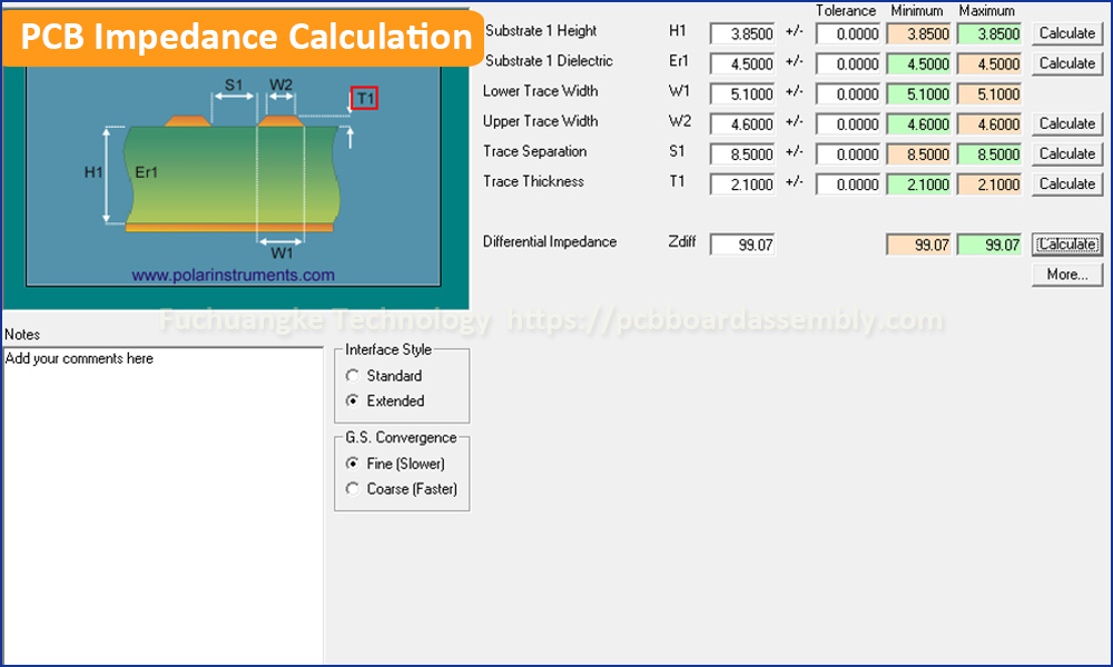
Differential Impedance is another commonly used impedance types in circuit board design and manufacturing. Differential impedance is the impedance between a pair of traces, also known as differential pair traces, when driven by equal and opposite polarity signals. From the Edge-Coupled Coated Microstrip type interfaces of Polar SI9000, we know the differential impedance is affected by many factors, including PCB substrate height, dielectric Er value, trace widths, trace separation (/spacing), trace thickness (/copper thickness), coating (/solder mask) thicknesses and coating dielectric. When handling differential impedance calculation, the main factors to decide the impedance is substrate height, Er value, trace width and spacing.
PCB Impedance Matching
The continual increase in device switching speeds is confronting PCB design engineers with signal integrity problems and eventually, most devices in the PCB fabrication and functional testing stage meet SI issues. That’s to say, PCB traces can no longer be treated as a simple point-to-point connection, but need to be considered as transmission traces ad impedance matching becomes necessary and required for ensuring no impact on SI.
PCB Impedance matching really features for your electronic and electrical devices to get best functions. Impedance matching is not normally required at low-frequency signals unless the mismatch between a trace and its upstream and downstream components is large.
Quick Quote
Click the Quick Quote buttons below, you can turn to the different PCB quote pages. Just fill in the PCB specifications, upload Gerber files, BOM, Assembly Drawing and Pick-and-Place file, you will get quick quote of PCB board and PCB Assembly.
FR-4 PCB Quote Flexible PCB Quote Rigid-Flex PCB Quote IMS PCB QuoteA professional PCB designer always do SI simulation before send his PCB Gerber files to the PCB manufacturer, but always ignore whether the PCB provider can supply the printed circuit boards with impedance matching your requirement. So, it seems very important to find a reliable and experienced PCB manufacturer. Finding no more, but Fuchuangke Technology, which is a Turnkey PCB and Assembly Manufacturer with 10+ years’ experience in circuit board manufacturing and PCB assembly. We can provide you the high-quality PCB boards meeting your expectations.