Do you know your PCB manufacturer and supplier always fabricate printed circuit boards on a large panel? Unless your PCB is large, or requires special processing, it’s likely it will flow through the PCB manufacturing process on PCB panels either only your PCB depending on the order quantity, or with a bunch of other PCB boards. The PCB assembly manufacturer will improve the SMT assembly efficiency through getting all your parts placed in one go without requiring any additional setup time. In another word, as a customer, you can save PCB Assembly cost with a PCB Panel.
Check to Know more PCB Panelizatin | PCB Panel
PCB Panel is required for SMT Assembly, but how to decide the Panel Size is important before panelizing no matter only with one design or a few, because too small or too large PCB in single boards or panel cannot be brought to the rails on the SMT lines. The panel size of PCB fabrication is different from that of PCB assembly. Here, it is worth mentioning to help you find out our PCB Panel Size of PCB assembly.
| PCB Assembly Panel | Size |
| Minimum | 48mm x 48mm (recommended) |
| Maximum | 250mm x 610mm (recommended) |
The smallest SMD component we can assemble is 01005 with SMD placement machines of Fuji NXT III high-precision, and we also support assemble components with fine pitch down to 0.4mm.
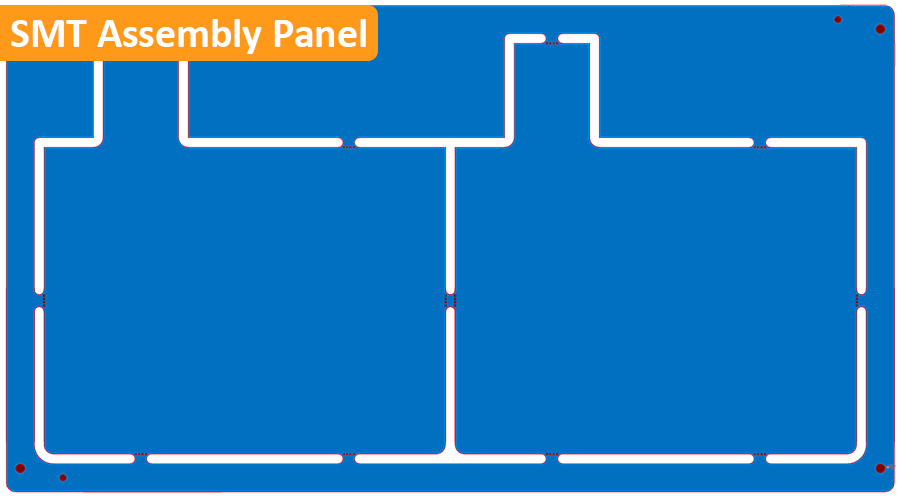
How to create PCB Panel?
If you want to produce PCB in high volume, it’s better to make PCB panel. You need to understand your PCB order is that the PCB producer builds only with your PCB design. And now, the PCB producer need to panelize your PCB in a big panel for the sake of high automation and repeatability to improve work efficiency and yield. The producer always goes as far as using both V-cut and Tab-routing methods simultaneously on a single PCB project. This combination of methods usually increases the cost of PCB production, but it reduces damages and reduce PCBA separating labor.
Single-up PCB Panel
Single-up PCB panel means only one design and one PCB board in the panel. Placing more PCB quantity on a panel is helpful for making production go much quicker. But there needs to be a balance. For an order with a low volume or prototypes, having panels be single-up is usually ok if that’s the fastest and cheapest way to get the PCB’s. But when order quantity goes into high volume or mass production, it would be best to really consider making the panels larger in order to improve the assembly process.
If the individual PCB’s themselves are large, then single-up panel may be necessary, regardless of the unit quantity ordered. For example, if the individual PCB is over 200mm then it’s likely that it would need to remain a single-up panel. However, if the PCB is under that, and the quantity is sufficient, then putting more PCB’s into a panel would be preferred.
Multi-up PCB Panel
Multi-up PCB Panel means only one design and a few boards in a panel. If the individual PCB is small such as 50mm, we can panelize a few, like 3 or 4 pcs, in the shorter edge to ensure the best PCB panel size. This multi-up PCB panel is applicable for Prototype PCB assembly and high volume. If the PCB is greater than 200mm in the long edge, we can multiple panelize a few PCBs on the short edge. But as always, the panel must still have 5-14mm waste-tabs around the edges with 3 fiducials on at least 2 waste-tabs and 4 tooling holes upon the actual SMT assembly requirement.
Waste-tabs on PCB panel edges
Waste-tabs, also called technique tabs, should be added to the PCB Panel. The waste-tabs with 5-14mm will increase the PCB cost of the Panel, but in some cases, it is worth the increasing cost. In high volume PCB assembly orders, the PCB assembly company would like to consider the cost savings of only adding waste-tabs on two edges of the Panel rather than all 4 edges. But this requires evaluation by our engineer on specific printed circuit board assembly project. The purpose of the waste-tabs around the Panel is to make sure that if there are any parts that hang over the edges, they have clearance from machinery, and board support if they are heavy or thin easy to break. If particular long connector is found in custom PCB assembly, the PCB assembly factory should extend the waste-tabs on that edge to be longer to support that extra part of the connector outside of the PCB edge.
In SMT assembly house, technicians or other people hold the PCBA on hand by hand through grabbing the PCB waste-tabs. Without anything to hold, it’s easy for fingers to get into solder paste or pre-reflowed, post-placement parts and thus ruin the product. What’s more, the waste-tabs enable us to use fixtures in whole PCB assembly and testing processes. For Flex Circuit Assembly, there is nothing to adhere the tape for fixtures. Besides, when the PCB requires 2 waste-tabs on the panel, adding waste-tabs on the long edge of the panel will be more economy than that on short edge.
Fiducials
- Fiducials Location: In cases with 4 waste-tabs around the PCB, fiducials should be added to the corners of the waste-tabs. These fiducials would be on the short length of the waste-tabs because almost all long edges of the PCB Panel are put on the rails of the SMT line. If adding fiducials on the long length, the fiducials may be covered by tools. But in cases of only 2 waste-tabs, fiducials can only be added on the long length, but need to keep enough distance from the very edge of the Panel to the center of the fiducials. What’s more, if the fiducials are located to the copper crossing, please remove the crossing, or the CCD camera of the pick-and-place machine can not read it, which will result that the components cannot be placed on correct pads or with bad alignment.
- Fiducial Quantity: PCB producer may add 4 fiducials on the waste-tabs, but the SMT Assembly Supplier would like to tell you that only need to add 3 fiducials, not 2 or 4 fiducials. Besides, fiducials should be added on both the top and bottom side. With 3 fiducials, the technician is easy to find out the PCB rotation.
- Fiducial Size: Fiducials should be 1mm in diameter with a 2mm masking area. They can be smaller or larger than this if necessary, but this is good of thumb and would be good to standardize on it.
- Tooling Holes: Tooling holes are very important but not cost any extra, especially for those PCB assembly requires support fixture and PCBA testing requires to contact the testing pads. PCB Assembly House always require 4 tooling holes with diameter 3.175mm (it was a standard pin support size) or 2mm in the corners of waste-tabs.
PCB Orientation in Panel
Individual PCB Orientation: Whenever possible all of the PCBs within the panel should be oriented (rotated) the same direction. When PCBs are rotated 180 degrees off from each other, it causes a considerable amount of extra work for programming of SMT machine and AOI machine. But in some cases, rotating the individual PCBs has some advantages, like reducing the panel size to save PCB cost, reducing the components threw rate to saving component cost.
FR-4 PCB Quote Flexible PCB Quote Rigid-Flex PCB Quote IMS PCB Quote