Electrical Test (E-test), which is the final electrical test to verify net continuity and the absence of shorts on the bare printed circuit boards (PCBs). In our PCB house, we perform 100% electrical testing on all bare PCBs its facilities as per IPC-9252 specifications.
Netlist File of PCB E-test
To test the PCB boards, we require the NETLIST file. Although we create a reference netlist from the customer’s original Gerber files during PCB fabrication, we always prefer to receive the CAD file based on the netlist for comparision. Since a CAD based netlist is generated before PCB routing, it provides another layer of checking (against the Gerber files). This allow us to catch any PCB faults intrducing in the event of an error in the Gerber files. For full turnkey PCB assembly projects, this helps to ensure that the PCB boards are 100% correct before any components are assembled. The preferred netlist format is IPC-356 since all CAD software package are capable of loading this format.
Our E-test Capabilities
| Min Continuity Resistance | 0.1 Ohms |
| Max Test Voltage | 1000 Volts |
| Max Isolated Resistance | 25 M Ohm – 2 G Ohm |
| Electrical Test Pitch (Fixture) | 20mil |
| Electrical Test Pitch (Flying Probe) | 4mil |
We have two different types of testing equipment available to test the fabricated circuit boards, including flying probe and fixture. When the order square less than 2sqm, we use flying probe method, when it’s more than 2sqm, we use fixture method. And we only charge one-time on E-test fixture cost, but flying probe E-test need re-charge in all orders. This E-test rule is applied in FR4 PCB, flex circuit and rigid-flex PCB and MCPCB.
Sometimes customers are unclear about the difference between Fixture (Bed of Nails) vs. Flying probe testing, as well as the costs associated with them. The following example will clarify the difference between the two methods, as well as the cases in which one or the other might yield a more efficient PCB Assembly Process.
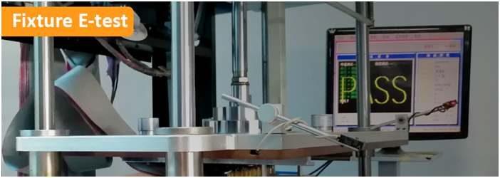
1. Fixture E-test
- Electrical Test Pitch = 0.020″
- Setup time: 30 minutes
- Learn time: 0 minutes
- Debug / check for missing pins: 10 minutes
- Test time per board: 40 seconds
- All points are tested simultaneously.
However, this process involves both setup time to create the fixture and additional costs associated with the cost of materials.
2. Flying Probe E-test
- Electrical Test Pitch = 0.004″
- Setup time: 0 minutes
- Learn time: 20 minutes
- Test time per board: 6 minutes
- The points are tested one at a time.
There is no setup time because the machine learns the program as it operates.
Bare PCB Testing
Bare PCB testing involves using capacitance and resistance tests. Each of the equipment uses a combination of both. Capacitance testing for a bare circuit board involves testing for opens and shorts by “charging” a net or plane and then probing each net to measure the induced capacity. Inaccuracies occur with this method because of the inherent variability in producing circuit boards. However, field measurement or field effect testing for shorts uses a very similar approach.
Resistance Testing
Resistance testing measures the resistance found in the net. As electric current flows through a conductor collision between electrons and atoms interfere with the flow of electrons. This is known as resistance and it is measured in ohms.
A good conductor has Low resistance – at common temperatures silver is the best conductor and copper is second. The amount of resistance depends on the conductor’s length and its cross-sectional area. If you have two circuits of the same material and the same cross-section and one is twice as long as the other -the longer one has TWICE as much resistance. If you have two circuits of the same material and the same length but one is twice as thick as the other -the thicker conductor will have HALF (Hot Air Levelling Lead Free) the resistance. So, resistance is proportional to length and inversely proportional to the cross-sectional area of a conductor and dissipates power in the form of heat.
Our test processes use CAD/CAM data for all test programs and optimize both ATG and trace test programs while meeting IPC Class II requirements. We follow the IPC 9252 specification guidelines for Class II testing processes, which means that we test 100% of the network on the PCB board for continuity and isolation (that’s opens and shorts) using a test program generated from your Gerber date. We do not test 100% of the points -we optimize out middle points of nets as allowed by the standard. We do not use your original Gerber data -it does not guarantee a 100% test.
What You Should Know about PCB Electrical Test
- 100% Net List Test: Check of every “node” on every net on the board.
- Adjacency Test: Type of test for checking isolation between conductors – shorts test. A software generated program that checks for nets that are within a tolerance set by the user. Two methods are used – Proximity Adjacency and Line of Site Adjacency.
- Clam Shell Test: Provides simultaneous testing of both sides of the board at the same time. These types of fixtures are used on single grid testers and dual grid testers. A very reliable method of bare board testing because all points are tested at the same time.
- Combined Grid/Probe Testing: Using the flying probe test sequence to cover areas of the board with fine pitch, high density points while the grid test verifies power to ground separation, through hole and wider pitch component pads.
- Comparative or Golden Board Test: Method using a “master” or known good board (KGB) to learn a program and then test other boards against the learned net list program. Poor choice for test accuracy – you may be learning a “bad” board.
- Continuity Test: Verification that the resistance between test points is lower than the specified limit or maximum continuity resistance. See shorts and opens tests.
- End of Net: A feature which is either the origin or the termination of a conductor network.
- Endpoint: A test point or node required to be tested to meet the 100% continuity and isolation test.
- Field Effect and Field Measurement Test: Refer to a type of test that uses large nets as antennas to send a specific high frequency alternating current at a specific voltage. The remaining nets are checked and those that have similar voltages for all antennas are considered as shorted and then retested using Ohm’s law resistance to verify the shorts.
- Flip Test: Consists of two separate, independent single sided tests on a universal grid. Testing one side and then the other. Unless a significant number of points are tested during both tests it can be a very inaccurate method.
- High Pot Test: Refers to high voltage potential testing to check for high resistance continuity or leakage between ground and power planes. DC voltages in the 500 to 1000 volt ranges are used for a specified dwell time.
- Impedance: The design of a circuit and the frequency of the current passing through it have various affects on the alternating current passing through it. The combination of these effects and the resistance of the conductor is called impedance.
- Impedance Control Test: A device called a TDR (Time Domain Reflectometer) is used to check circuits to determine if they are within expected tolerances. Conductor length, spacing, width, height and separation affect the impedance.
- In Circuit Test: Test performed after components are installed – a check for shorts or opens caused during assembly operations.
- Isolated Land: A test point not connected to any other test point or net. Also called a single point net, singlet or no connect.
- Isolation Resistance: The resistance tolerance between the circuit board’s non-connected traces and/or lands.
- Land: A portion of a conductive pattern usually used for connection, component attachment or both. Surface mount pads, component hole pads, gold fingers etc.
- Leakage: Movement of current between two conductors that are not connected and therefore should be isolated by a minimum amount of resistance. Causes significant “noise” in the properties of the circuit board.
- Middle Net Point: A feature which is a not at either the termination or origin of an interconnecting network
- Net: An entire string of points or connections from the first source point to the last target point including lands and vias.
- Net List: A list of alpha-numeric locations, used to describe a group of two or more points that are electrically common.
- Node: A connection point between a network and an off- the-board item like a component or test probe. See Land
- Opens Test: Check to make sure there is current flow from one “node” to the next for every net on the board, again by measuring the amount of resistance of the conductor.
- Optimized Net List Test: Check every “end of net” for all nets on the board and selected intermediate nodes on the board.
- Shorts Test: Check to make sure that NO current flows between separate nets by measuring the amount resistance between them.
FR-4 PCB Quote Flexible PCB Quote Rigid-Flex PCB Quote IMS PCB Quote