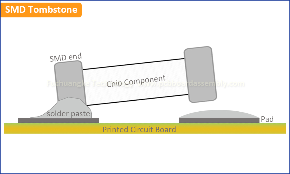
SMD Tombstone in Reflow Soldering
If you are in the SMT assembly manufacturing industry, you should know the SMD tombstone problem is caused by the force imbalance at the both end of the multilayer chip components during reflow soldering, but do you know how many reasons can lead to an imbalance in wetting force? This PCB blog elaborates the causes and mechanisms behind tombstoning.
What’s Tombstone?
Tombstone (also known as the Manhattan effect, drawbridge effect, or PCB tombstoning) is a passive chip component assembly defect. One metalized end of a passive component, such as a chip resistor or capacitor, rises up out of solder and breaks contact with the pad, while the other end is attached and soldered onto another pad.
What’s Tombstone Mechanism?
Before reflow soldering or solder paste melt, due to the action of the gel in the solder paste, both ends of the component are fixed t the PCB pad by the adhesive force (f), and by the gravity (G) by itself, the SMD component doesn’t move or rise up when the PCB moves forward on the conveyor.
Weldability Testing Experiment.
- In the first half of T0 phase, the measured force is negative since the surface tension of the liquid solder paste is at work. In this period, the paste has just melted but not wetted the component metalized end surface, the liquid surface tension will produce a buoyancy upward to push the component, so that the force measured by the instrument is reduced compared to the component weight.
- After the second half of the T0 phase, the solder begins to wet the component metalized end surface, the measured wetting force began to be positive from negative. When the solder completely wetted the component metalized ends, the wetting force also reached the maximum and no longer increase, to a stable state.
- If the solder on the both PCB pads doesn’t welt the two metalized ends of the component at the same time, i.e. the rate difference between the two ends of wetting is large, or the two ends of the wetting force gap is large, then a new effect will occur: the left end of the component with solder wetting will produce a left wetting force, while the right end’s solder does not wet, the surface tension of the molten solder will produce an upward buoyancy force on the component. The wetting force will produce a counterclockwise rotational torque (FL1) with fulcrum O, at which point the component is subject edged by three torques, wetting FORCE FL1, gravity GL2 and buoyancy FL3 (counterclockwise). When the torque produced by the wetting force and buoyancy is greater than the torque of gravity, the component will rise up and then stand. Of course, if the wetting forces on both sides are not the same, then the right side will also produce the same left-hand wetting torque (clockwise). When FL1 is greater than the sum of the wetting torque of GL2 and the right side, the component in reflow soldering will occur tombstone or offset.
In the tombstone troubleshooting process, we find the tombstone places are mostly chip capacitors or inductors, rarely resistors. This can actually be seen from the shape structure of the component, the chip capacitor or inductive end face is usually square, the height value is larger, and the resistance is basically a smaller rectangular shape. In the wetting process, the wetting force arm L1 of square capacitance or inductance is certainly greater than resistor with the same size. Assuming that the wetting forces are the same, the force arm is large and the torque is large, and the effect is more obvious. That’s why the tombstone possibility of SMD resistor is relatively small.
What Are the Reasons of SMD Tombstone?
According to the mechanism of the chip component tombstone, the cause of the tombstone also needs to be analyzed from the reason of the uneven wetting force at both ends of the component. In the actual SMT PCB assembly production process, there are many reasons may lead to uneven wetting at both ends, but not all the reasons will certainly cause tombstone, we will see what are these reasons? The reasons to tombstone are far more than the below said, but not all of them will certainly lead to tombstone.
- The coating solderability of two ends of the component is poor. If the two ends have weldable differences, wetting capacities are not the same, which will produce two different wetting force torques, may occur poor wetting, offset or tombstone problems. If one end is not wetting at all, tombstone will occur.
- The tin paste deposition volume on two pads are big difference, so the tin paste melting temperatures are big difference, and the melting rates are big difference. It may occur offset or tombstone problems, but which are not generally easy to occur, after all, the stencil mesh opening difference will not be too big.
- Tin paste printing bias. If the tin paste printing is offset and not fully deposited on the pad, which leads to one or two ends can’t be effective contact with the solder paste, like no contact or a small amount of contact. This is very likely to offset or tombstone problems.
- The areas of the two pads are with different design. The design difference may lead to two problems. (1) Different pad sizes affect the flow of melting solder paste on pads. (2) Heat absorption and heat dissipation rates of the two pads are not the same, i.e. the pad temperature rising under the two pads are different, which will lead to the difference of tin paste melting rate and wetting. Both of them may cause offset and tombstone problems.
- The solder mask dam between the two pads is higher than the two pads. The component placed onto the two pads may not flat, and when the solder paste is melting, one side of the two ends will occur tombstone.
- The big pad gap between the two pads. You can see it in many PCB designs. If the gap is large, the possibility to tombstone is big.
- There is solder paste on the area between two ends. The solder paste between them will be melt and rise up the component and occur tombstone problem.
- The SMD placement pressure is insufficient in pick-and-place process. The component cannot be effectively exposed to the paste, which may cause the component tombstone during transmission.
- Inadequate precision in placement may also lead to the tombstone, the paste cannot be fully in contact with the two ends of the component, resulting in wetting differences between the two ends, the tombstone or offset may occur.
- Profile problem. If the heating rate is too fast, the temperature rising and the heat distribution is uneven on the PCB board, which leads to tombstone.
Quick Quote
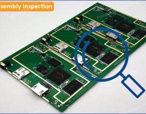
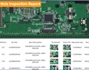
Click the Quick Quote buttons below, you can turn to the different PCB quote pages. Just fill in the PCB specifications, upload Gerber files, BOM, Assembly Drawing and Pick-and-Place file, you will get quick quote of PCB board and PCB Assembly. We provide SPI, AOI, X-ray, FAI and FCT value-added services to ensure highly reliable PCB assemblies.
FR-4 PCB Quote Flexible PCB Quote Rigid-Flex PCB Quote IMS PCB Quote